
Silicon wafers are pivotal components in the semiconductor industry, forming the foundation for integrated circuits in electronic devices. The careful handling and storage of these wafers within semiconductor facilities are critical processes that directly influence product quality and performance.
In this comprehensive guide, we will explore essential practices for handling and storing silicon wafers in semiconductor facilities, emphasizing efficiency and risk mitigation to uphold the highest standards of quality and reliability.
In semiconductor fabrication, cleanroom environments are meticulously controlled to minimize contamination risks and guarantee the highest quality of silicon wafers. These environments typically adhere to strict cleanliness standards, such as ISO Class 1 or Class 10 cleanrooms, where the number of airborne particles is meticulously controlled per cubic meter of air.
Cleanrooms have specialized filtration systems that continuously remove particles from the air to maintain optimal conditions. High-efficiency particulate air (HEPA) filters and ultra-low particulate air (ULPA) filters capture particles as small as 0.3 microns and 0.12 microns, respectively.
Electrostatic discharge poses a significant threat to silicon wafers during handling and storage. Semiconductor facilities implement static control measures such as grounding straps, ionizing air blowers, and conductive flooring to dissipate static charges and prevent damage to wafers.
Personnel wears ground straps to safely discharge static electricity from their bodies while ionizing air blowers neutralize static charges on surfaces. Conductive flooring materials allow static charges to dissipate harmlessly to the ground, reducing the risk of electrostatic discharge events.
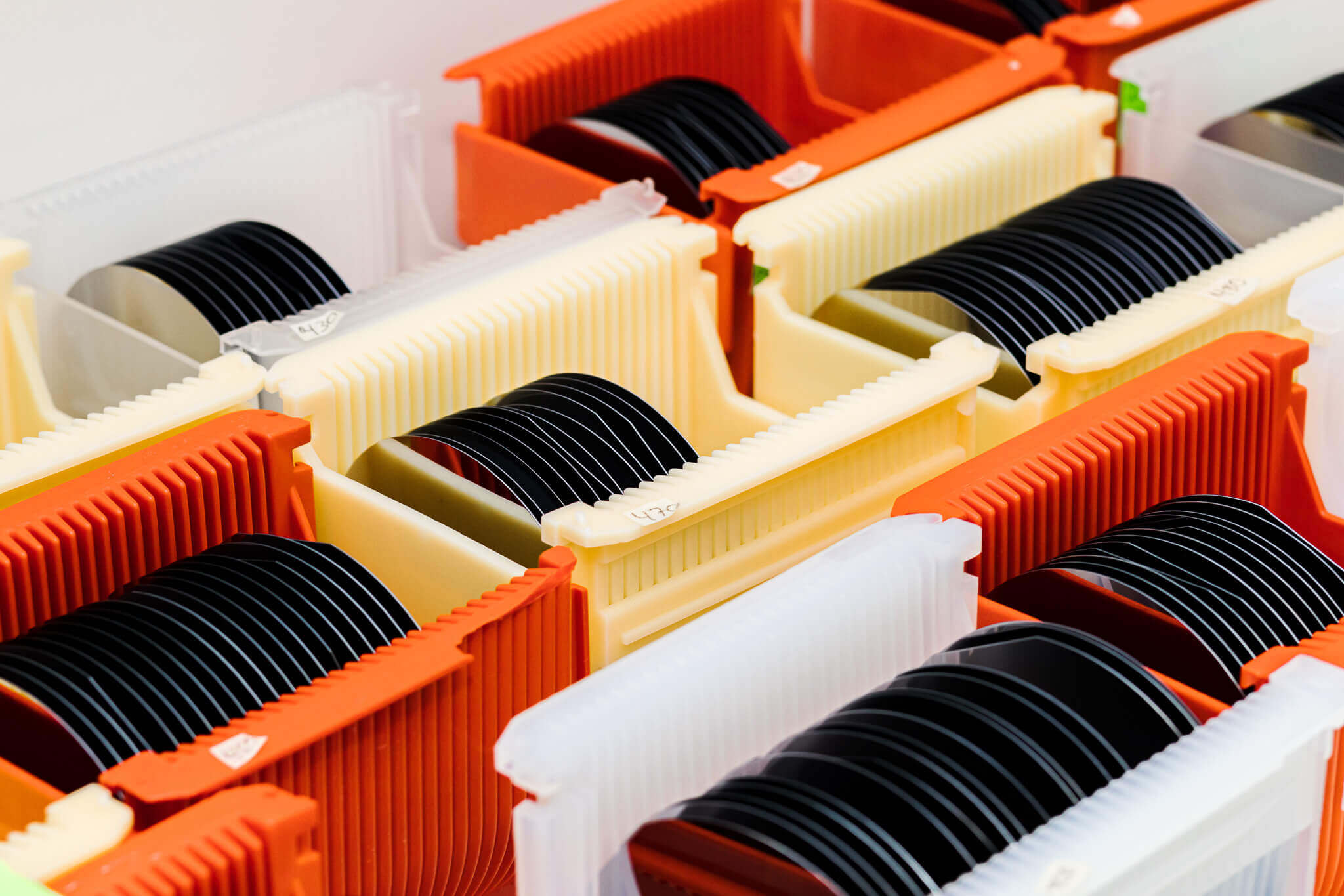
Proper packaging is vital for protecting silicon wafers from physical damage, contamination, and moisture during transit and storage. Semiconductor facilities use various protective packaging solutions to safeguard wafers and maintain their integrity throughout the supply chain.
One common packaging solution is vacuum-sealed packaging, where silicon wafers are placed in a sealed pouch or container and vacuum-sealed to remove air and create a protective barrier against contaminants and moisture. Desiccant packs are often included in the packaging to absorb residual moisture and maintain a dry environment.
Strict adherence to handling protocols is essential to minimize risks during wafer fabrication and assembly. Semiconductor facilities develop detailed handling procedures and protocols that outline best practices for safely transporting, manipulating, and processing silicon wafers.
These handling protocols typically cover a wide range of activities, including wafer loading and unloading, wafer inspection, chemical processing, and mechanical manipulation. They provide step-by-step instructions for each task, specifying the equipment to be used, the proper techniques to be followed, and the safety precautions to be observed.
Robust identification and tracking systems provide accountability and traceability throughout the semiconductor manufacturing process. These systems assign a unique identifier to each silicon wafer, containing information about its origin, processing history, and quality inspection results.
One common wafer identification method is using barcodes or radio-frequency identification (RFID) tags, applied to wafers at various stages of manufacturing. These identifiers are scanned and recorded at each step of the production process, allowing semiconductor facilities to track the movement and status of wafers in real-time.
Proper storage conditions are critical for maintaining the quality and integrity of silicon wafers throughout the semiconductor manufacturing process. Semiconductor facilities maintain dedicated storage areas within cleanroom environments, equipped with climate-controlled cabinets and racks to preserve wafers under optimal conditions.
Temperature and humidity control are essential for preventing degradation and ensuring the stability of silicon wafers during storage. Semiconductor facilities typically maintain storage temperatures between 18°C and 22°C and humidity levels between 40% and 60% to minimize the risk of moisture-related damage and contamination.
Efficient inventory management is crucial for semiconductor facilities to meet production demands while minimizing excess inventory and associated costs. Advanced inventory management systems play a vital role in optimizing supply and demand dynamics by providing real-time visibility into inventory levels, usage rates, and demand forecasts.
These systems utilize sophisticated algorithms and analytics to analyze historical data, market trends, and production schedules, enabling semiconductor facilities to accurately forecast demand and adjust inventory levels accordingly. Automated reorder alerts and inventory optimization tools help streamline procurement processes, ensuring timely stock replenishment to avoid production delays or shortages.
Continuous improvement initiatives are vital for driving innovation and excellence in semiconductor manufacturing. These initiatives focus on identifying opportunities for improvement, implementing changes to optimize processes, and fostering a culture of continuous learning and innovation.
One common approach to continuous improvement is the use of lean manufacturing principles, such as value stream mapping, Kaizen events, and 5S methodology. These principles emphasize the elimination of waste, the standardization of processes, and the empowerment of employees to identify and address inefficiencies in their work environments.
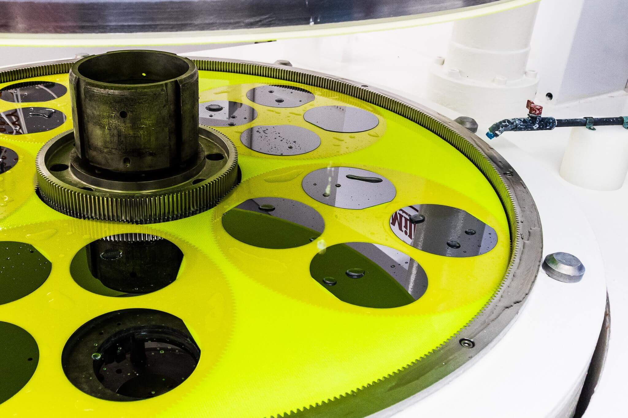
Rigorous quality control processes are essential for ensuring flawless performance in semiconductor manufacturing. These processes involve the systematic inspection, testing, and validation of silicon wafers to detect and address any deviations or defects that may impact product quality and reliability.
One common quality control process in semiconductor manufacturing is the use of automated inspection systems, such as optical scanners and surface analysis tools, to inspect wafers for defects and imperfections. These systems use advanced imaging techniques and algorithms to detect anomalies in wafer surface morphology, thickness, and composition, ensuring only wafers that meet predefined quality standards proceed to the next stage of production.
Environmental sustainability is a growing priority in semiconductor manufacturing, driven by a commitment to minimize environmental impact, conserve natural resources, and promote responsible stewardship of the environment. Semiconductor facilities implement a variety of eco-friendly practices to reduce energy consumption, minimize waste generation, and mitigate environmental pollution.
One common environmental sustainability practice in semiconductor manufacturing is the use of energy-efficient equipment and processes to reduce energy consumption and greenhouse gas emissions. Semiconductor facilities invest in energy-efficient lighting, heating, and cooling systems and process optimization technologies, such as advanced process control and wafer-level optimization, to minimize energy use and improve overall operational efficiency.
Employee health and safety are paramount concerns in semiconductor facilities, where workers are exposed to various hazards associated with wafer handling and storage. Stringent health and safety protocols are enforced to safeguard employees from potential risks, including chemical exposure, ergonomic injuries, and cleanroom-related hazards.
One key aspect of employee health and safety protocols is the implementation of comprehensive training programs to educate employees on the risks associated with their work and provide them with the knowledge and skills needed to perform their jobs safely. Training programs cover topics such as chemical handling and exposure control, ergonomic best practices, cleanroom safety procedures, and emergency response protocols, ensuring that employees are equipped to identify and mitigate hazards in their work environments.
Semiconductor facilities are subject to a wide range of regulations and standards governing wafer handling and storage practices. Compliance with these regulations and standards is essential for maintaining the integrity, safety, and legality of semiconductor manufacturing operations and avoiding potential legal and financial liabilities.
One key area of regulatory compliance in semiconductor manufacturing is environmental regulations, which govern the handling, storage, and disposal of hazardous materials and waste. Semiconductor facilities are required to comply with regulations such as the Resource Conservation and Recovery Act (RCRA), the Clean Air Act (CAA), and the Clean Water Act (CWA), as well as state and local environmental regulations, to minimize environmental impact and protect public health and safety.
Effective silicon wafer handling and storage are critical for maintaining product quality and reliability in semiconductor facilities. By implementing these essential practices, facilities can optimize efficiency, minimize risks, and uphold quality standards, driving innovation and excellence in the semiconductor industry.
Wafer World has top-notch wafers you can order! Contact us today!


