Compliance with high-quality standards is important in the industry of silicon wafer manufacturing. These standards serve as the foundation for ensuring the stability and performance of silicon wafers in a wide range of applications, including microelectronics and solar cells. In this article, we will peel back the layers of industry standards for silicon wafer suppliers, providing light on the critical function of quality testing and how it is methodically carried out.
Quality Standards in Silicon Wafer Manufacturing
Industry Standards for Silicon Wafers: A Comprehensive Overview
The semiconductor business, which is driven by constant innovation and the need for increased performance, relies on well-defined standards to maintain uniformity and interoperability. The International Electrotechnical Commission (IEC) and Semiconductor Equipment and Materials International (SEMI) are two well-known organizations that develop standards for silicon wafer technology.
IEC Standards: The IEC is a key player in developing worldwide standards for electronics and associated technology. The IEC specifies silicon wafer size, materials, and quality parameters. These standards assure homogeneous wafer qualities, allowing for interoperability across a wide range of applications.
SEMI Standards: SEMI is a multinational industry group dedicated to the creation of standards for the microelectronics manufacturing supply chain. SEMI standards address a wide range of areas, including wafer fabrication, packaging, and handling. They provide a complete framework for promoting uniformity and efficiency in the production process.
Dimensional Standards: Dimensional accuracy is crucial in silicon wafer production. Standards specify the diameter, thickness, and flatness tolerances. This precise control over dimensions is required for seamless connection with technological devices.
Material Quality Standards: Silicon wafers are made from high-purity silicon ingots. The standards define allowable levels of impurities, crystalline flaws, and contamination. Maintaining strict material quality standards is critical to ensuring the dependability and lifetime of electronic components.
Importance of Quality Testing: Guaranteeing Reliability and Performance
Quality testing is the cornerstone of silicon wafer manufacturing, acting as a gatekeeper to guarantee that each wafer fulfills the required specifications. The value of quality testing spans across multiple dimensions.
Reliability Assurance: Quality testing is the first line of defense against faults that may jeopardize the dependability of electronic products. It detects and eliminates wafers with structural or material flaws, preventing potential failures in finished products.
Performance Optimization: Silicon wafers designed for a variety of applications require precise performance characteristics. Quality testing confirms essential factors like resistivity, carrier lifetime, and surface properties. This optimization assures that the wafer meets the performance requirements of the intended application.
Cost-Efficiency: Identifying and correcting faults early in the production process is important for both quality and efficiency. Quality testing reduces the manufacture of faulty wafers, lowering material waste and production costs.
Customer Satisfaction: Meeting or exceeding quality standards demonstrates a manufacturer's dedication to excellence. Consistent delivery of high-quality silicon wafers builds customer trust, increases satisfaction, and creates long-term relationships.
How Quality Testing is Conducted: A Step-by-Step Guide
Quality testing in silicon wafer production is a laborious procedure that uses a variety of tools and methodologies to properly inspect each wafer.
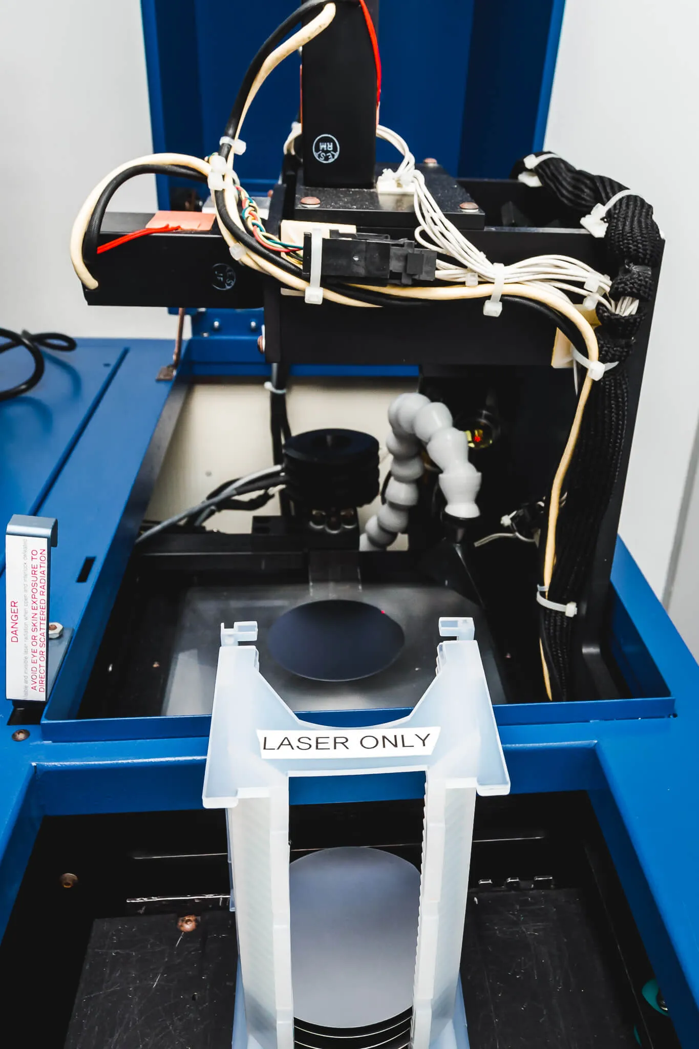
Visual Inspection: The procedure begins with a visual inspection to detect surface abnormalities, fissures, or contaminants. Advanced imaging technologies enable high-resolution examination, allowing for the rapid detection of obvious faults.
Dimensional Measurement: Precision is critical in semiconductor production. Automated measurement instruments are used to determine the diameter, thickness, and flatness of each wafer, assuring dimensional conformity.
Material Analysis: To determine the chemical composition of the wafer, advanced analytical techniques including mass spectrometry and spectroscopy are used. This aids in the identification of contaminants and guarantees that material quality standards are met.
Electrical Testing: Each wafer is rigorously checked to verify that it has suitable electrical properties. This involves determining resistivity, carrier concentration, and mobility. These tests guarantee that the wafer's electrical properties match the planned application.
Defect Detection: Advanced inspection instruments, such as scanning electron microscopes, are used to detect minute faults in the crystal structure. This degree of examination helps to eliminate wafers with flaws that could jeopardize performance.
Wafer Mapping: Wafer mapping is the systematic testing of several spots on the surface of each wafer. This comprehensive method guarantees that variations in attributes are identified and corrected, hence contributing to overall consistency.
Final Verification: The final stage entails comparing all metrics to the stated standards. Only wafers that meet or surpass these specifications are considered suitable for further processing and integration into electrical devices.
Adaptation to Technological Advances
As technology advances, so do expectations for silicon wafers. The use of innovative materials, such as silicon carbide and gallium nitride, creates new obstacles and opportunities. Quality standards must adapt to reflect these developments, ensuring that the production process meets the specific needs of these sophisticated materials.
The emergence of 3D semiconductor architectures and heterogeneous integration necessitates a review of current standards. The traditional focus on planar silicon wafers needs to be broadened to include the complexities of vertically stacked systems, demanding revisions to dimensions and material quality standards.
International Collaboration for Global Consistency
Collaboration is essential in today's global business. Harmonization of standards across regions promotes consistency in silicon wafer manufacturing, allowing for easy integration into a wide range of electronic products around the world. Organizations such as IEC and SEMI play critical roles in bringing stakeholders together to produce universal standards that cross geographical boundaries.
Maintaining global consistency benefits manufacturers reassures end users, and improves supply chain efficiency. It's a wealth of shared knowledge and mutual understanding that keeps silicon wafer quality high across a wide range of applications and industries.
Looking for Silicon Wafer Suppliers? Contact Us Today!
In the ever-changing world of silicon wafer production, adhering to industry standards and rigorous quality testing is more than a habit; it is a commitment to perfection. As silicon wafers continue to constitute the foundation of modern electronics, quality standards become increasingly important. Wafer World must remain committed to preserving these standards, ensuring that each silicon wafer contributes to the smooth operation and dependability of the gadgets we rely on every day. Call us today to purchase!