.webp)
Stay up-to-date with the latest news and trends in wafer and semiconductor technologies.
*Blogs are for educational and informational purposes ONLY
The key differences between Sapp, gallium arsenide, and silicon carbide wafers in modern electronic applications.
Read More
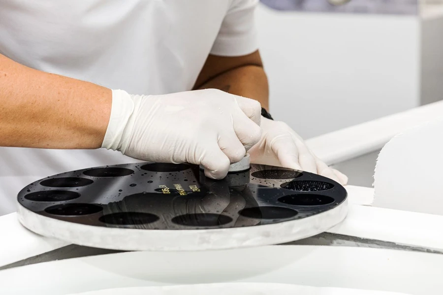
Silicon carbide reclaim technology advances wafer reuse, improving sustainability, reducing waste, & supporting manufacturing.
Read More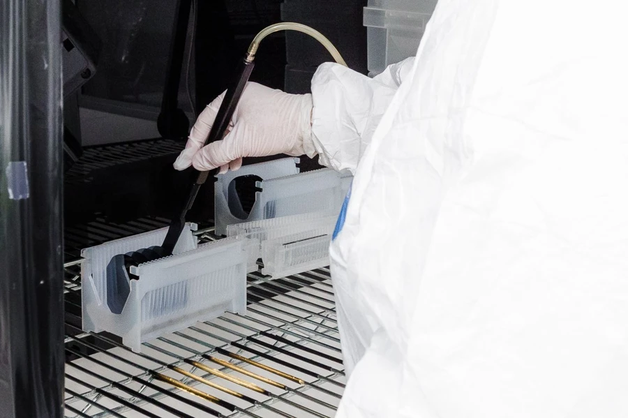
Explore practical tips for protecting ultra flat wafers from contamination, breakage, and environmental exposure.
Read More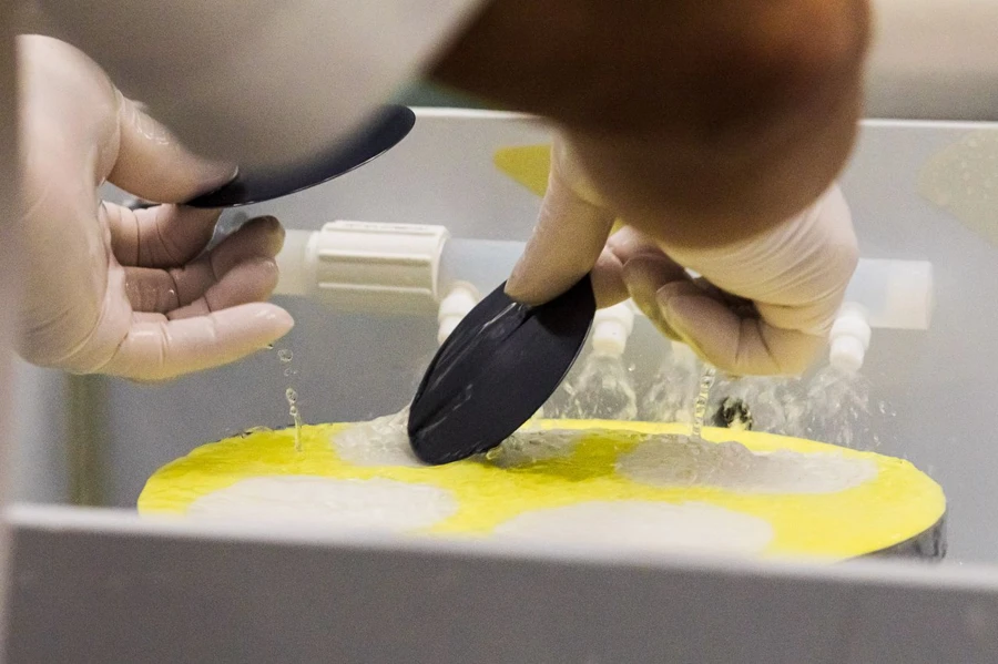
SiC wafers shape modern electronics, from heat management to voltage performance and long-term stability.
Read More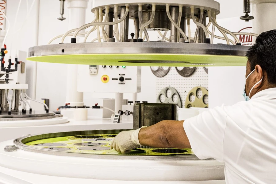
Silicon wafer processing innovations improve precision, yield, surface quality, and reliability for advanced semiconductor needs.
Read More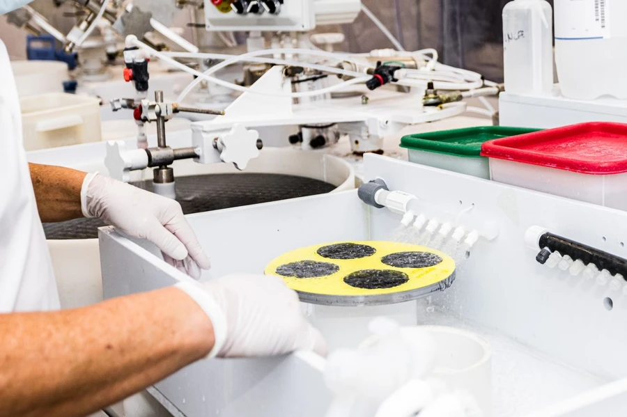
Here’s how InP wafers enable faster optical communications, advanced sensing, data centers, & next-generation photonic devices.
Read More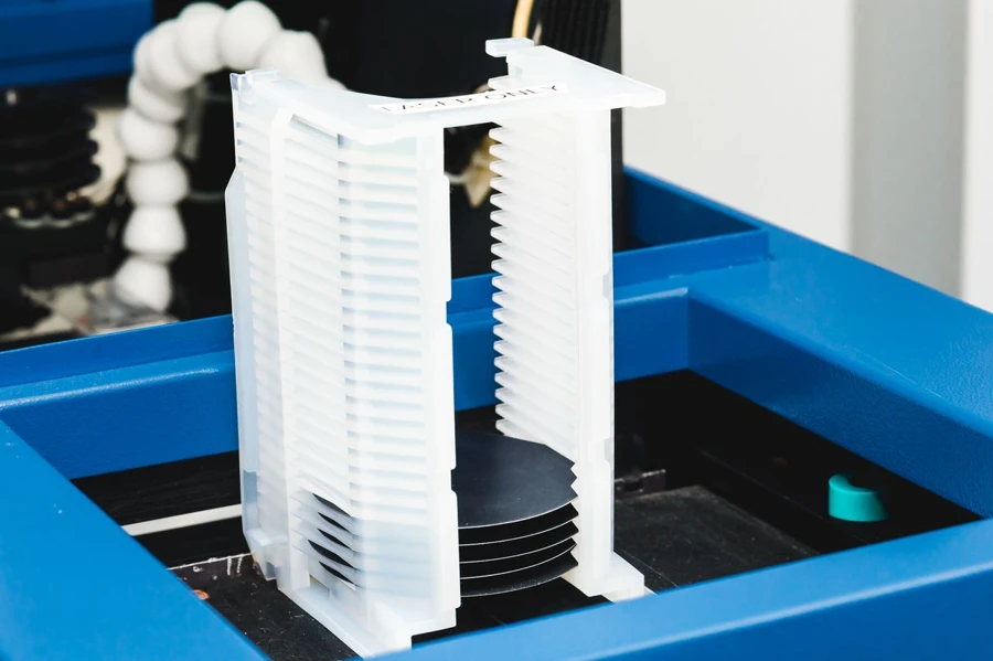
Here’s why material quality is essential for silicon wafer Manufacturers seeking reliable performance, consistency, and yield.
Read MoreLearn how FZ wafers are manufactured, key production challenges, and what impacts wafer quality in high-precision semiconductor applications today.
Read More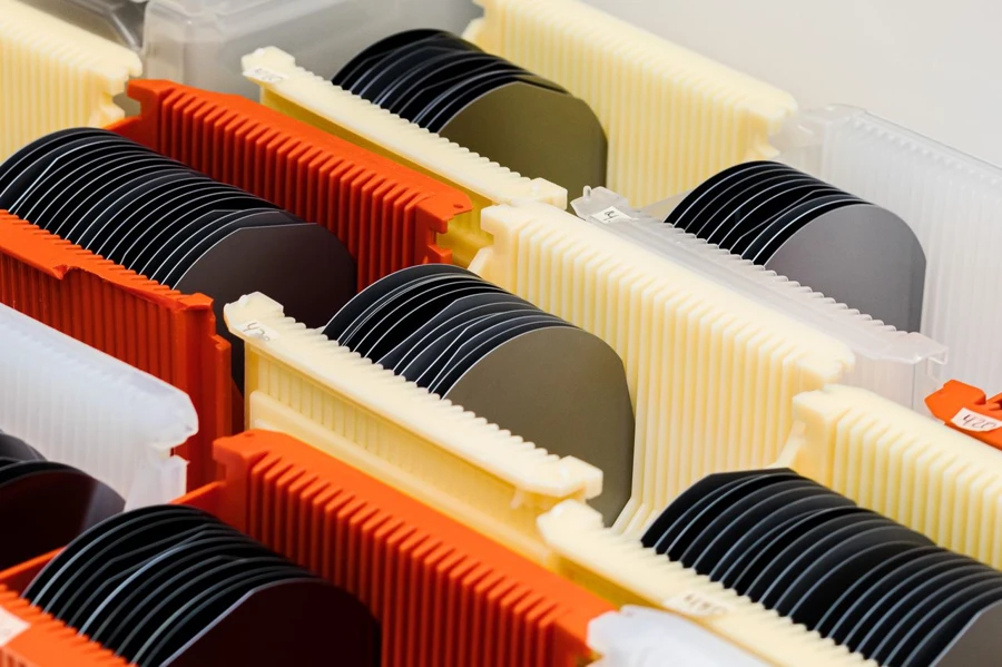
Supply chain factors influence silicon prices, affecting availability, production costs, and market stability worldwide.
Read More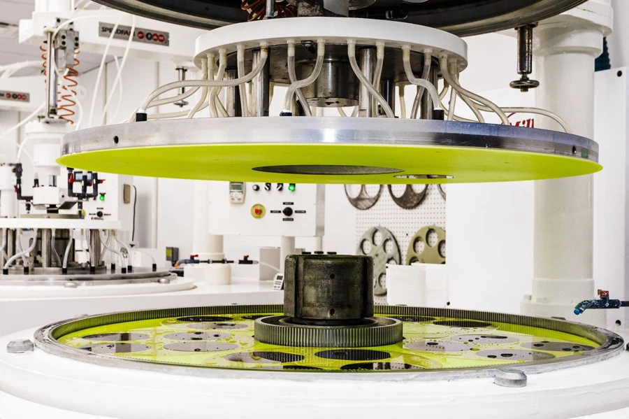
Automation is transforming silicon wafer manufacturing through improved precision, quality control, efficiency, and yield.
Read More