Indium phosphide is a compound used to manufacture semiconductors with a single crystal structure. The structure’s stability makes an InP wafer the go-to choice for applications involving telecommunications and microwave technology, particularly in fiber-optic communication systems.
However, InP wafer adoption isn’t widespread yet, and this is mainly due to common challenges during manufacturing.

InP has a low melting point (1062°C). This, combined with phosphorus volatility, makes crystal growth complex. Phosphorus pressure must be carefully controlled to avoid decomposition during growth.
The phosphine (PH₃), used in epitaxy and doping, is extremely toxic and pyrophoric. Wafer fabs need to follow stringent safety protocols and isolated fabrication environments. Additionally, managing waste and exhaust systems is a must to prevent environmental contamination.
InP has a specific lattice constant, so epitaxial layers must be carefully lattice-matched to avoid strain and defects. This makes heterostructure growth (for lasers and photodetectors, for example) more difficult than on silicon.
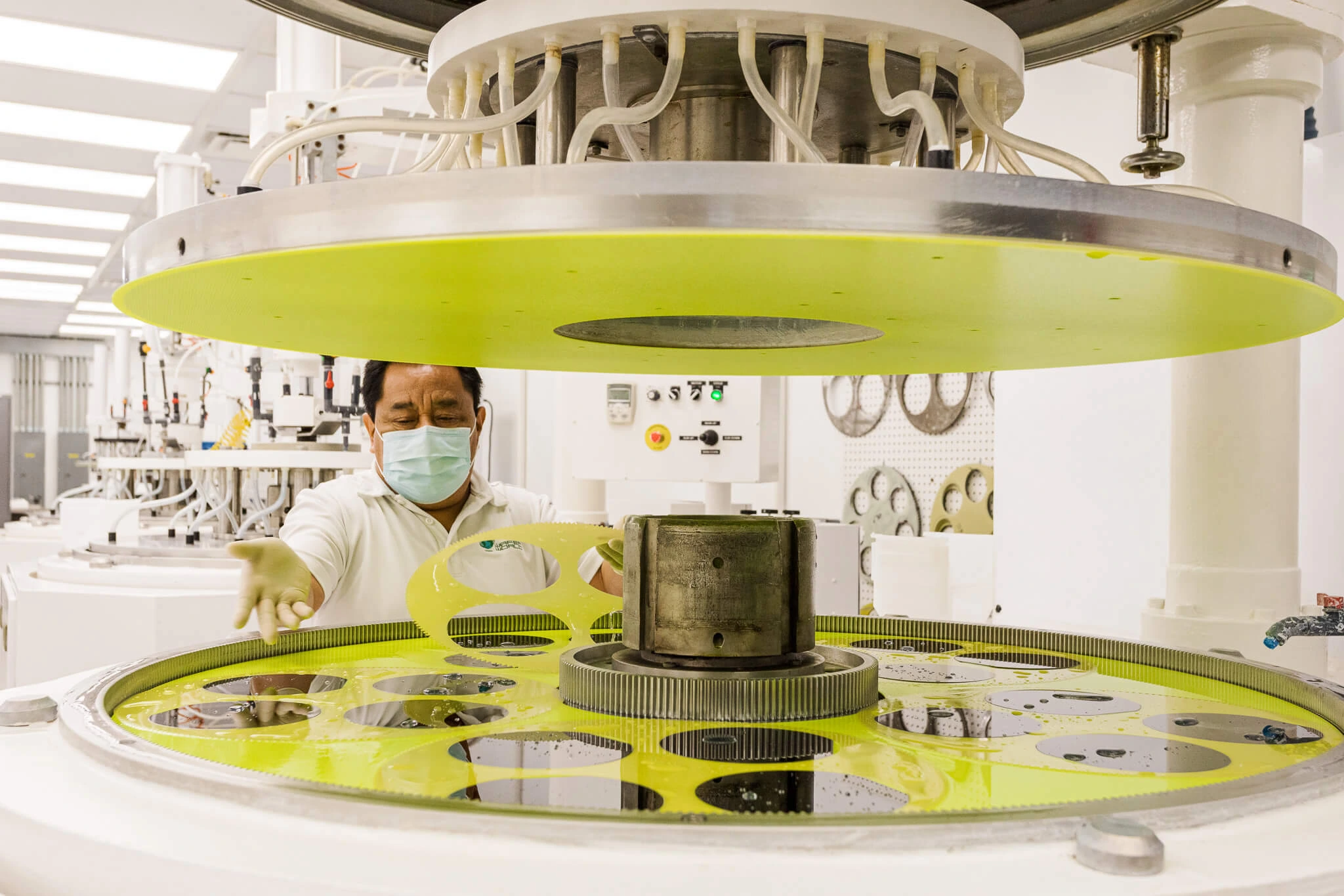
InP wafers are brittle and more prone to cracking than silicon wafers. Handling and processing (cutting, polishing, thinning) require extreme care and often specialized tools.
Lower thermal conductivity than silicon makes heat dissipation harder during device operation and thermal processing, which must be done at lower temperatures to avoid degradation.

Due to the material's physical, chemical, and thermal properties, creating an indium phosphate (InP) wafer involves several technical challenges. In addition to being challenging during manufacturing, InP wafers can be hard to dope.
Particularly, p-type doping is difficult to perform uniformly. Zn and Fe are commonly used dopants, but controlling their concentration and diffusion is more difficult than silicon.
This affects the wafer’s cost and availability, as InP substrates tend to be much more expensive and less available than silicon or even GaAs wafers. If you’d like to explore a more economic alternative to brand-new InP wafers, our reclaimed InP wafers offer all the beneficial properties for a lower price.
Contact Wafer World today for more information!


