Packing GaAs Wafers

Packing GaAs Wafers: Requirements and Complications

Author:

August 4, 2025

Shop Now

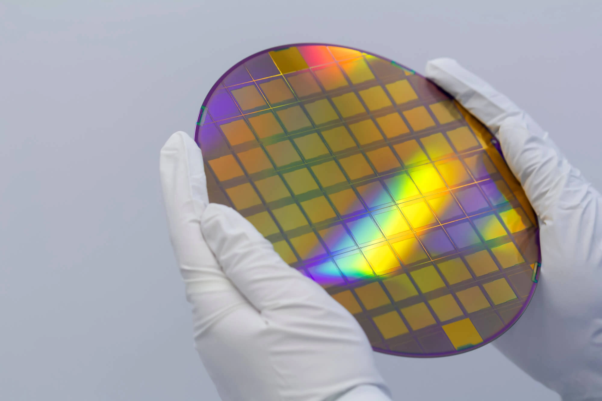
Gallium arsenide is a unique compound for semiconductors. Its direct bandgap, present even in GaAs reclaim wafers, makes them particularly useful in optical devices because photons, the basic unit for all light, can easily pass through lenses.

However, GaAs is not perfect. This material is more brittle than silicon, and after the reclaim process, it can be even more so—meaning specialized packing techniques are crucial to protect its integrity.

5 Specialized Packing Techniques for GaAs Wafers

  • Vacuum-sealed or Nitrogen-Purged Containers: These containers protect against oxidation, moisture, and contaminants. They’re a common option for epitaxial GaAs wafers or wafers with sensitive surface treatments.
  • Cushioned Wafer Carriers or Gel Packs: These consist of plastic containers with individual slots or gel-based holders that minimize mechanical shock and vibration. They prevent sliding or contact between wafers.
  • Anti-Static Materials: Use ESD-safe carriers and anti-static foam if electrostatic discharge is a concern.
  • Cleanroom Packaging: Double-bagged in cleanroom-safe polymer bags.
  • Temperature and Shock Considerations: To prevent damage during shipping, outer packaging may include shock-absorbing foam, temperature insulation, or rigid boxes.

Understand How to Transport GaAs Reclaim Wafers Safely

GaAs is more brittle than silicon, making it prone to cracking, chipping, or breaking during handling and transport. To make matters worse, this semiconductor material can release arsenic compounds if damaged, making it a risk for those transporting and working with it. Understanding the best packing techniques is key to preventing that.

At Wafer World, we produce brand-new and reclaimed GaAs wafers, so we’re experienced in shipping them. If you’d like to learn more, contact us today!

Wafer World Banner