July 23, 2025
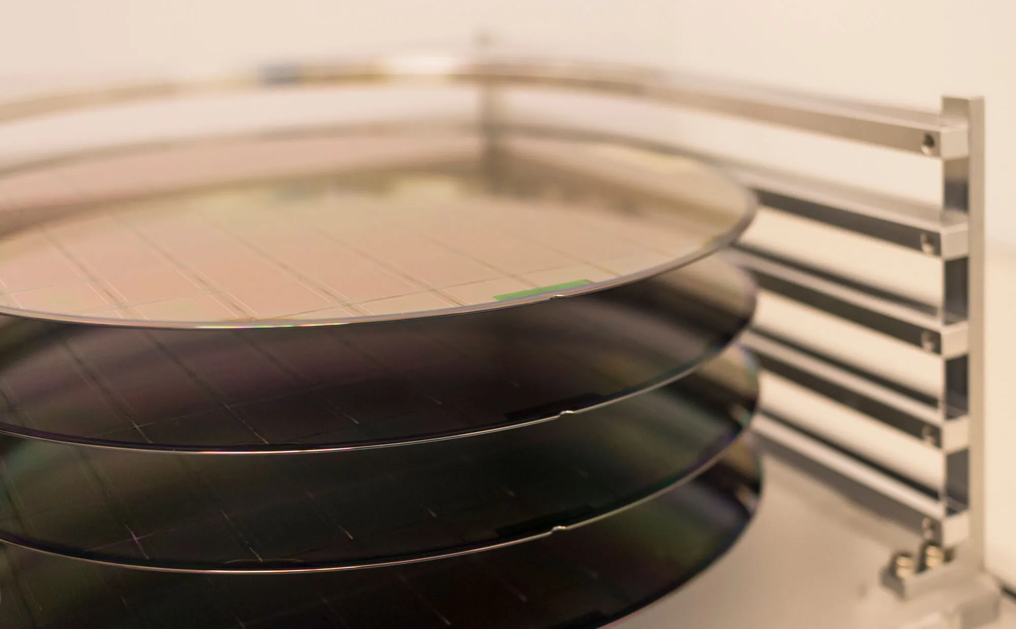
Shop NowInP reclaim wafers allow manufacturers to make processes more efficient, protect the environment, and enjoy all the benefits of indium phosphide at half the cost. However, reclaiming this material is both expensive and technically demanding, so manufacturers carefully screen wafers before deciding if they’re worth the effort.

Manufacturers begin with a visual inspection using optical or laser-based inspection tools to spot noticeable issues. This includes:
Once no issues were identified, the semiconductor's bow and warp are measured using tools like laser interferometers. Thickness is checked to ensure the wafer won’t fall below the minimum usable limits after grinding.
If the wafer is already too thin or warped beyond specification, it’s discarded.
Then, the surface is analyzed using AFM (atomic force microscopy) or ellipsometry to assess roughness and detect subsurface damage (from previous CMP or etch steps). X-ray diffraction (XRD) may be used to check for crystalline damage.
If damage goes too deep, reclaiming would require excessive grinding, risking wafer breakage or excessive thinning.

The reclaim process offers several benefits, but conducting it carelessly can be expensive and often fruitless. At Wafer World, we do considerable testing and inspection before putting them through the reclaim process to ensure the quality of our wafers.
In addition to all of these steps, we keep track of each wafer's history. A wafer that has already gone through several reclaim cycles often needs to be discarded. If you’d like to learn more about the quality of our products, contact us today!


