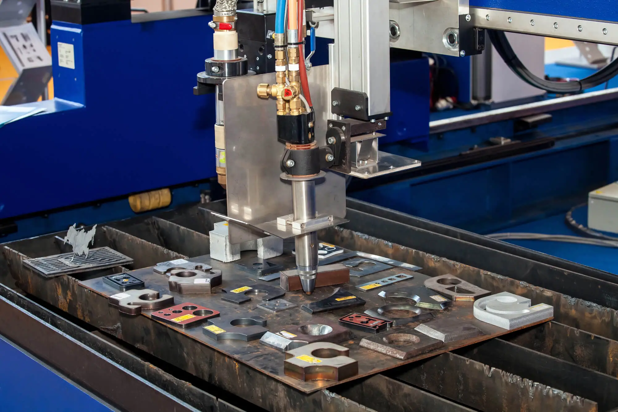
Laser marking is a non-contact, precise process used by wafer manufacturers for labeling and tracking products. Unlike traditional marking methods, this efficient alternative employs a laser beam to alter the surface of a material, leaving a visible mark.
Among its tasks, the three main purposes of laser marking are engraving, annealing, and ablation. This last step removes material from the substrate, leaving marks such as 2D codes or unique identifiers.
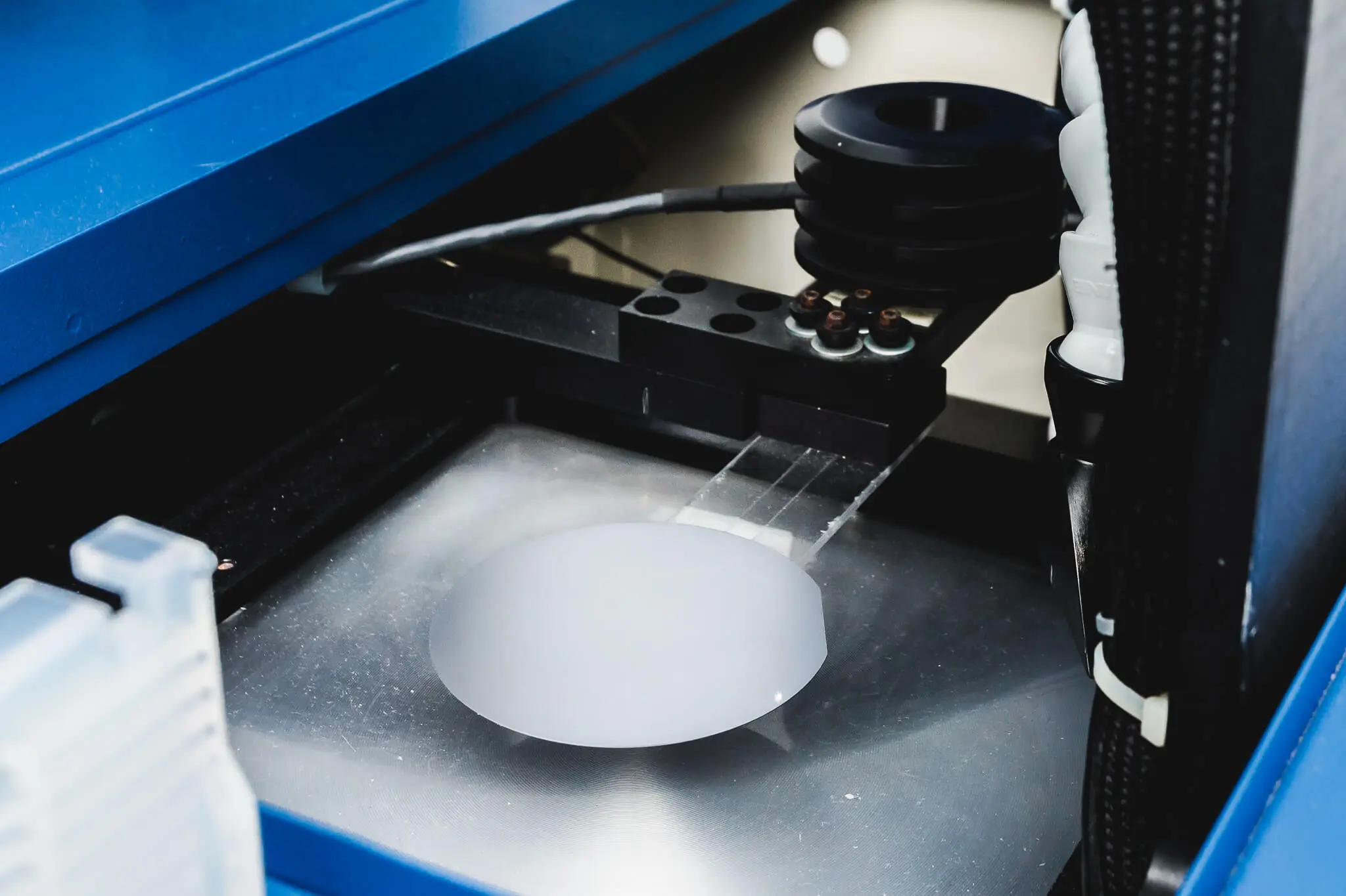
Ablation is a laser marking method that uses vaporization or evaporation to remove material from the silicon wafer's surface. The laser energy heats the material rapidly, causing it to vaporize, sublimate, or eject in fine particles.
Because of its high level of control, this process can remove material precisely without harming the surrounding areas.
The silicon material absorbs the laser energy, which causes it to heat up and vaporize quickly. It can be used to create shallow or deep markings because the depth of the ablation can be precisely controlled, and the controlled removal of material leaves a visible mark.
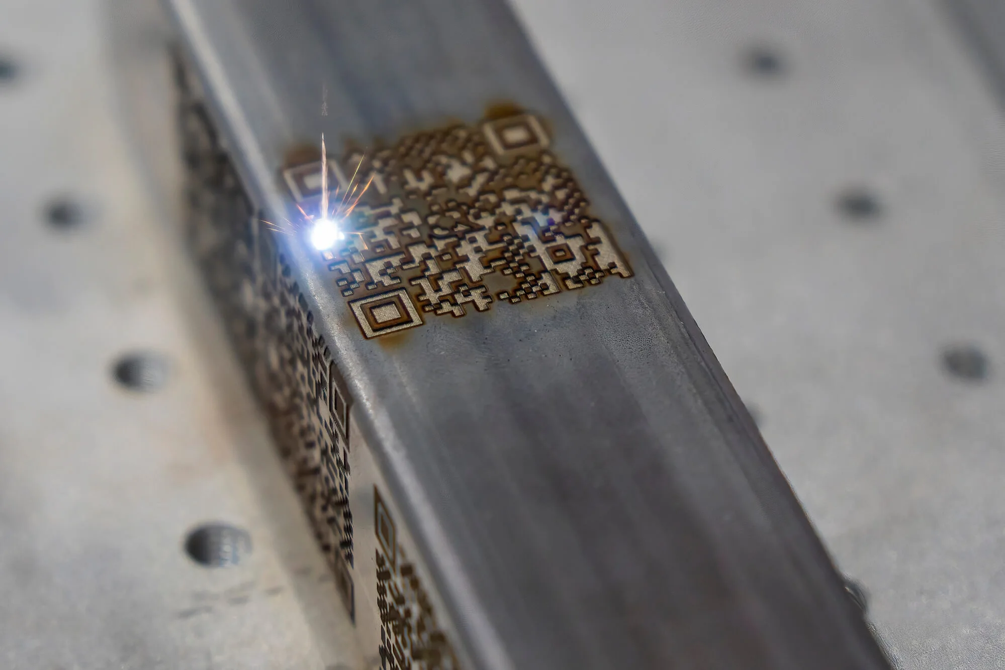
Ablation is the method of choice for high-density information marking on silicon wafers due to its accuracy and low thermal impact. It can be especially helpful for applications like 2D codes or unique identifiers that require marks with different depths.
Here at Wafer World, we laser mark all our products to follow industry standards and optimize back-office processes. If you’d like to learn more, give us a call!


