%20(1).webp)
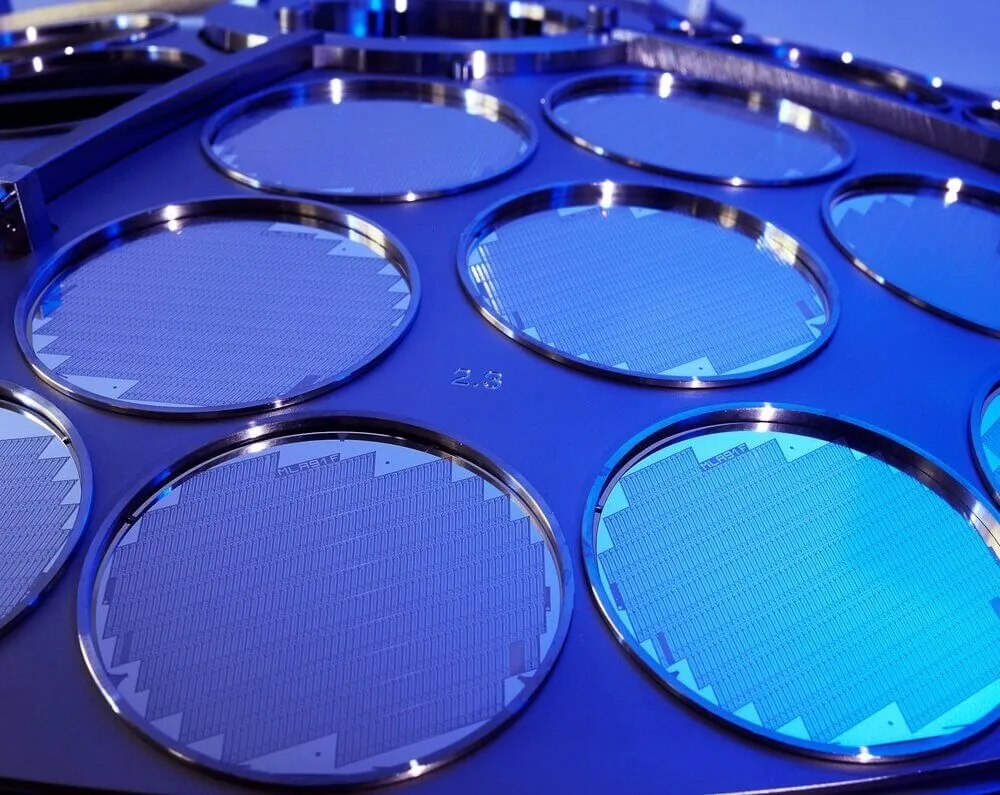
In the ever-evolving landscape of semiconductor manufacturing, precision and efficiency are paramount. Laser marking has emerged as a versatile and indispensable tool in the arsenal of techniques used for silicon wafer identification and traceability. In this exploration, we delve into the intricacies of laser marking techniques—specifically engraving, annealing, and ablation—and examine their profound effects on silicon wafers.

https://www.youtube.com/watch?v=nNxbWcNgF2s&ab_channel=WaferWorldInc.
Before delving into the techniques, let's first understand what laser marking entails. Laser marking is a non-contact process that employs a laser beam to alter the surface of a material, leaving a visible mark. This technique is widely used in the semiconductor industry to label and identify silicon wafers, providing an efficient and high-precision alternative to traditional marking methods.
Engraving stands out as one of the primary laser marking techniques employed on silicon wafers. This method involves removing material from the surface of the wafer to create a visible mark. High-powered lasers, such as fiber lasers or UV lasers, are commonly used for engraving due to their ability to deliver focused and intense beams.
The process begins with the laser beam interacting with the silicon wafer's surface. The energy from the laser is absorbed by the material, causing localized heating and subsequent vaporization or melting. The controlled removal of material leaves a permanent, high-contrast mark on the surface.
Engraving is particularly useful for creating intricate and detailed markings, such as serial numbers, logos, or alphanumeric codes. The precision offered by this technique ensures legibility and durability, crucial for traceability throughout the semiconductor manufacturing chain.
Unlike engraving, annealing is a laser marking technique that relies on controlled heating to produce a visible mark without physically altering the silicon wafer's surface. This method is well-suited for applications where preserving the material integrity is essential.
In annealing, the laser beam heats the surface of the silicon wafer to a temperature below its melting point. This controlled heating induces a change in the material's crystalline structure, resulting in a color change visible to the naked eye. The coloration is often a result of oxidation or the formation of a thin oxide layer on the surface.
One significant advantage of annealing is its ability to create high-contrast, legible marks without compromising the structural integrity of the silicon wafer. This makes it ideal for applications where maintaining the material's physical properties is crucial, such as in microelectronics or MEMS (Micro-Electro-Mechanical Systems).
Ablation is a laser marking technique that involves removing material from the silicon wafer's surface by vaporization or evaporation. This process is highly controlled, allowing for precise material removal without causing damage to the surrounding areas.
The laser energy is absorbed by the silicon material, leading to rapid heating and vaporization. The controlled removal of material results in a visible mark, and the depth of the ablation can be precisely controlled, making it suitable for creating shallow or deep markings.
Ablation is particularly useful for applications that require varying depths of marks, such as 2D codes or unique identifiers. The precision and minimal thermal impact of ablation make it a preferred choice for high-density information marking on silicon wafers.
Laser marking techniques contribute significantly to the optimization of semiconductor manufacturing workflows. The non-contact nature of laser marking reduces the risk of contamination and damage to delicate silicon wafers. This is especially critical in cleanroom environments where even the slightest impurity can impact the performance of microelectronic devices.
Engraving, annealing, and ablation can be strategically applied at different stages of the manufacturing process. For example, initial wafer identification can be achieved through laser engraving, ensuring clear and durable marks for subsequent processing steps. Annealing may be employed for more intricate markings, while ablation could be utilized for high-density information or unique identifiers.
Each laser marking technique has distinct effects on silicon wafers, and the choice of technique depends on the specific requirements of the application.
Selecting the appropriate laser marking technique depends on the specific needs of the application and the desired outcome. Here are some key considerations:
.webp)
As semiconductor technology advances, the demand for precision in manufacturing processes continues to grow. Laser marking techniques—engraving, annealing, and ablation—stand at the forefront of this drive for precision in silicon wafer identification and traceability. Each technique brings its unique advantages, offering semiconductor manufacturers a versatile toolkit to meet the demands of diverse applications.
Whether it's creating intricate logos with engraving, preserving material integrity through annealing, or achieving precise material removal with ablation, the world of laser marking on silicon wafers opens up new possibilities for innovation and efficiency. As the semiconductor industry evolves, mastering these laser marking techniques becomes not just a necessity but a pathway to achieving the pinnacle of precision in manufacturing. Contact us to order!


