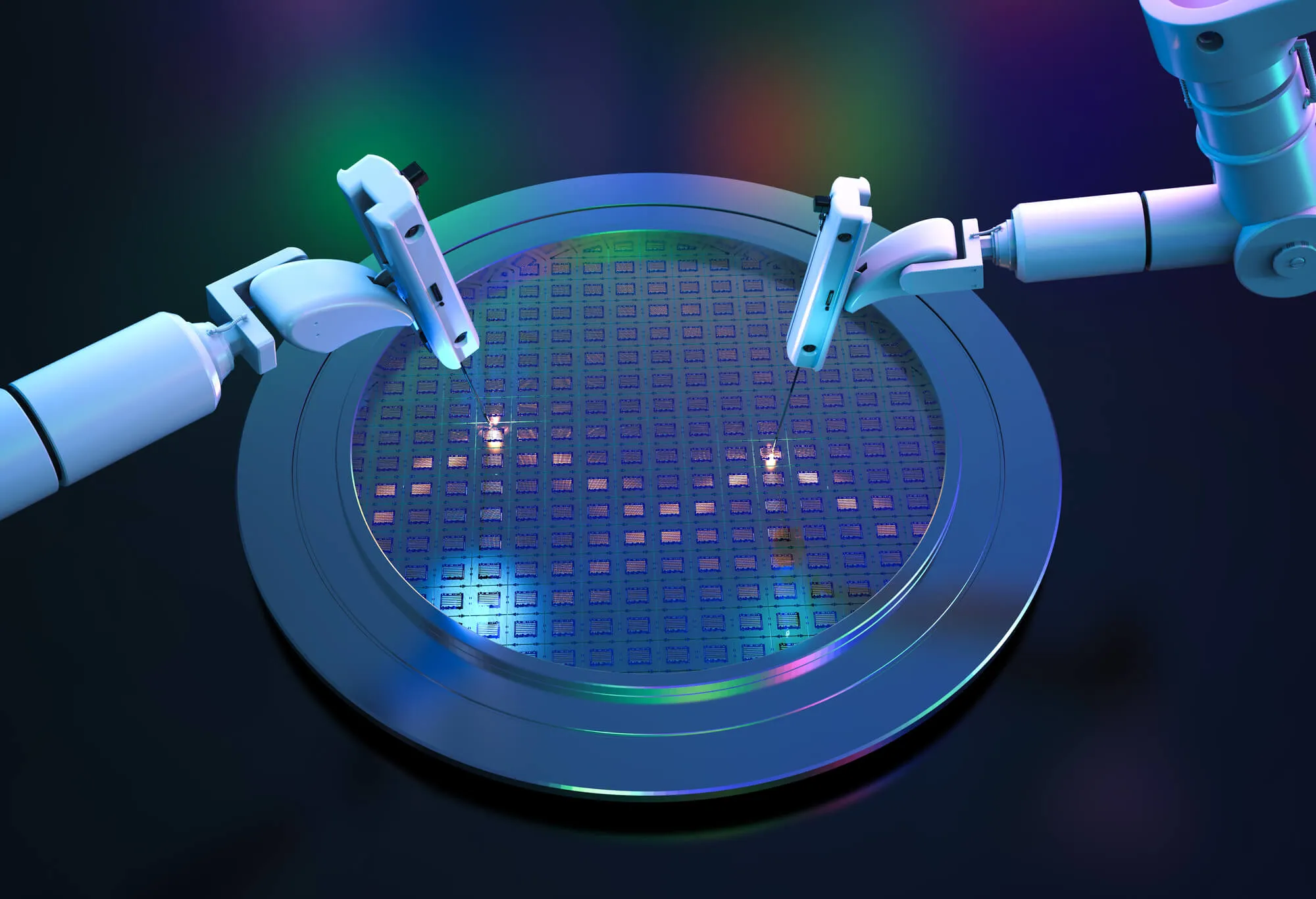
Wafers and printed circuit boards (PCBs) require traceability throughout the entire manufacturing process. For this reason, manufacturers use laser marking systems that produce miniaturized and machine-readable marks without negatively affecting the semiconductor manufacturing process.
Unlike traditional marking methods, this superior technology creates precise and accurate markings on micro-components in just a matter of seconds. In most cases, these markings are less than a millimeter in size. The laser marking machine preserves the wafer’s structural integrity because the laser doesn’t strip away anything from its surface during the marking process.
.jpg)
Wafer manufacturers ensure the entire process chain’s traceability by printing each wafer’s lot number on the wafer’s surface. However, lot numbers are arranged through holes that tend to accumulate around the pits.
Failure to address the accumulation issue increases the likelihood of producing defective wafers. Since laser marking systems create markings without creating hard and excessive protrusions that leave scratches on the surface of the wafer, they’re the ideal wafer marking solution.
A circuit module called an integrated circuit (IC), or a chip, integrates electronic components on a silicon board to accomplish a specific function. The chip’s surface features patterns and numbers for identification and other procedures. Since chips are high in integration density and small in size, they require high-precision laser marking machines.
Laser marking machine technology uses the laser’s thermal effect to leave a clear and permanent mark on the surface of the chip without damaging its components. Besides being pollution-free, this non-contact processing technique produces faster results than traditional electrochemical and mechanical marking methods.
.jpg)
Whether you’re looking to learn more about laser marking technology or you need high-quality wafers at a reasonable price, Wafer World has you covered. Don’t hesitate to get in touch with us today to get a free quote!


