November 20, 2023
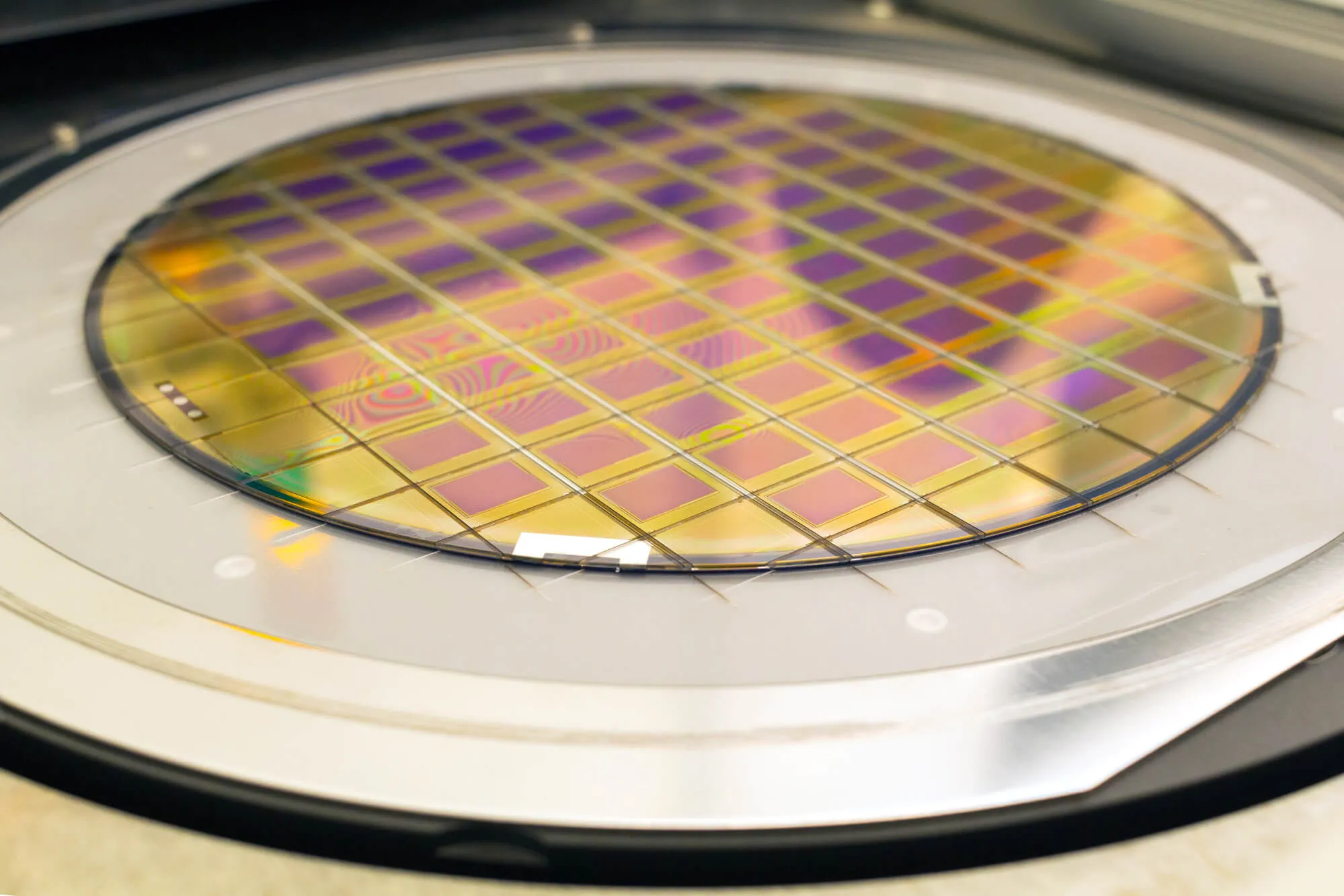
Shop NowPrecision and dependability are critical in the complex world of semiconductor fabrication. Semiconductor wafers, the foundation of microelectronics, go through several processes before becoming the heart of the electronic devices we use every day. Among these operations, laser marking is critical for assuring traceability, quality control, and compliance.
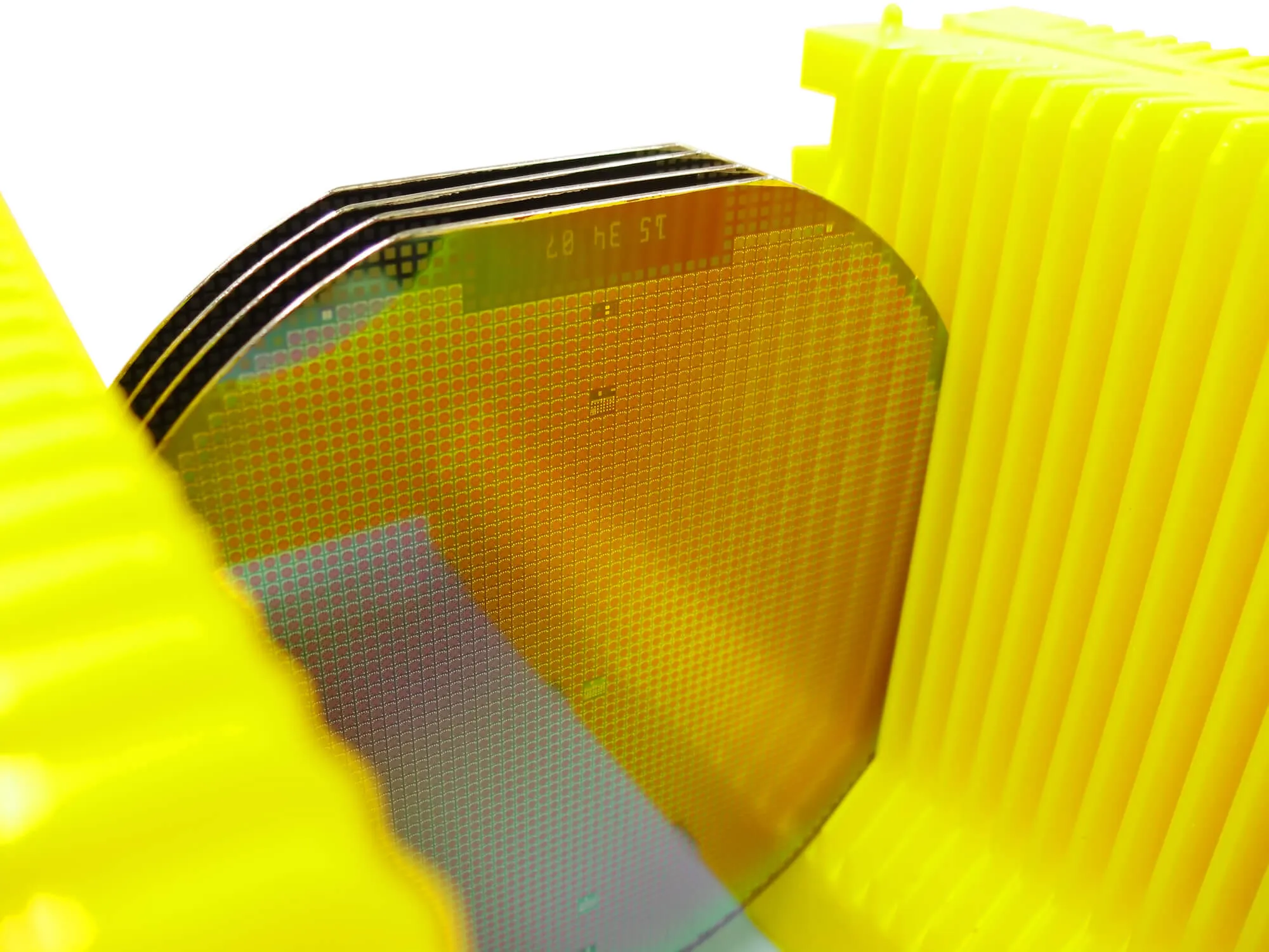
Laser marking technology offers unparalleled precision. It enables manufacturers to create microscopic, indelible marks on semiconductor wafers. These marks carry vital information such as serial numbers, production dates, and barcodes. The permanent nature of laser marks ensures that critical data remains intact throughout the life cycle of the semiconductor device.
In the semiconductor industry, compliance with regulatory standards is non-negotiable. Laser marking ensures that each wafer is uniquely identified, facilitating traceability from fabrication to final assembly. This traceability is instrumental in addressing potential defects and recalls and maintaining consistent product quality.
In an age of counterfeit electronics, laser marking acts as a powerful deterrent. Manufacturers can incorporate special markings and holograms that are almost impossible to replicate. These measures protect consumers from substandard or fake electronic components.
Laser marking helps maintain the highest quality standards. By marking wafers with vital information, manufacturers can track the performance of individual wafers throughout the production process. This information allows for the removal of defective wafers, ensuring only the highest quality devices reach consumers.
Laser marking is not just about marking wafers; it's also about data. Integrating laser marking into Industry 4.0 practices means real-time monitoring, data collection, and analytics, leading to more efficient production processes and predictive maintenance.
In the world of semiconductor manufacturing, laser marking is far more than a mere technicality. It's a linchpin that ensures product authenticity, quality, and regulatory compliance. It exemplifies how precision technology is reshaping the industry, one wafer at a time.
With Wafer World, you are sure that laser marking is a big part of our process! Call us today!


