
June 26, 2023
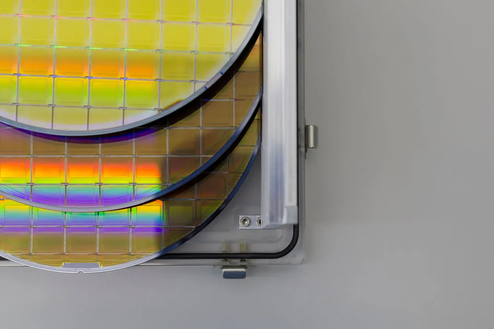
Shop NowMicroelectronics and semiconductor production require extreme precision and accuracy. Three techniques are commonly used to mark wafers: laser marking, etching, and engraving. While they may appear the same, each method has distinct advantages and is best suited to specific applications.
In this blog post, a Silicon Wafer Supplier will discuss the differences between laser marking, laser etching, and laser engraving and the benefits and drawbacks of each in wafer processing with a Silicon wafer supplier.
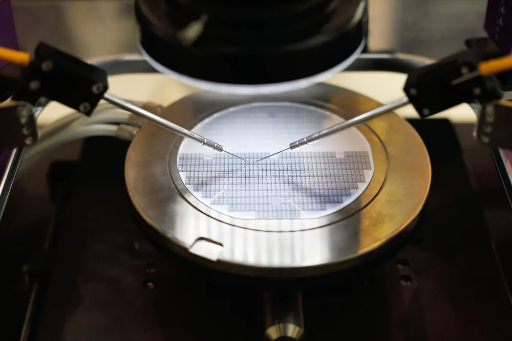
In the semiconductor business, laser marking is a popular method for marking wafers with various types of information. This non-contact approach uses high-energy laser beams to permanently mark the surface of the wafer. Laser marking is a precise and efficient method with various advantages for wafer applications.
Because of its amazing precision and accuracy, laser marking is suitable for producing complicated designs, small letters, and high-resolution graphics on wafers. The concentrated laser beam's precise details ensure the marks are visible, readable, and well-defined. This level of accuracy is crucial for traceability applications like stamping wafers with barcodes, alphanumeric identifiers, and serial numbers.
Since laser marking is a non-contact procedure, the laser beam does not physically contact the wafer's surface. This eliminates the chance of mechanical damage or contamination, preserving the structural integrity and cleanliness of the wafer. As a result, laser marking is ideal for fragile or sensitive materials such as silicon, which is widely used in the semiconductor industry.
Laser marking is appropriate for high-volume manufacturing situations due to its fast-processing speeds. Rapid marking increases overall efficiency by simplifying production lines and shortening cycle times. The ability to quickly mark wafers allows for efficient throughput and meets modern semiconductor manufacturing demands.
Laser marking is compatible with a variety of wafer materials, including silicon, metals, ceramics, and polymers. Because of this versatility, manufacturers can use the same laser marking technology to label wafers of varied materials. Laser marking is a versatile solution for wafer processing because of its ability to label a wide range of materials without losing quality or performance.
Laser marking systems integrate easily into automated manufacturing lines. They can be programmed to identify wafers automatically, eliminating the need for manual handling and reducing the potential for errors or inconsistencies. Laser marking and automation improve wafer processing efficiency, precision, and reproducibility.
In the semiconductor industry, laser etching is a process used to generate indented or raised structures on the surface of wafers. Compared to laser marking, it involves the controlled vaporization of the substance using a higher energy laser beam. Laser-etching offers numerous benefits and is well-suited for specific wafer processing applications.
When compared to laser marking, laser etching produces deeper patterns on the wafer surface, resulting in greater visibility and contrast. The deeper etchings create a clearer and more visible imprint, making it ideal for applications that require excellent readability. The increased difference ensures that the marks can be distinguished even in low-light conditions.
Laser etching works with a variety of wafer production materials, including silicon, metals, and ceramics. Because of this adaptability, many types of wafers can be marked with the same laser etching equipment. Laser etching on a hard or soft wafer is a reliable and precise method for creating indented or raised patterns.
Marks created by laser etching are particularly resistant to wear and tear. The vaporization of the material during the etching process results in deep, permanent marks that remain visible over time. Because laser-etched marks are long-lasting, they can withstand the rigors of semiconductor manufacturing processes such as cleaning, handling, and packaging.
Laser etching on wafers can reproduce high-resolution graphics and complex designs. This function is beneficial in applications that require etching complex patterns, logos, or symbols onto the wafer surface. The ability to make visually appealing and informative marks requires the ability to achieve fine details and exactly duplicate visuals.
Laser engraving is a highly precise and versatile wafer processing procedure that removes a significant percentage of material from the wafer's surface. It uses a high-powered laser beam to ablate the material, resulting in deep, permanent, and precise engravings. Laser engraving has several advantages, and it is beneficial in applications requiring three-dimensional effects or tactile identification.
Laser engraving creates three-dimensional effects on the wafer surface by generating deep grooves, holes, or channels. The ability to deeply etch the material allows for creating textured surfaces, enhancing visual appeal and functionality. Depending on the application, these textured surfaces may be used for greater grip, increased adhesion, or decorative purposes.
Laser-engraved marks are extremely durable and resistant to erosion. Eliminating a significant amount of material ensures that the engravings remain readable and unaltered even when subjected to harsh environmental conditions or subsequent manufacturing methods. The deep and permanent nature of laser engraving provides long-term wafer identification and traceability.
Laser engraving has excellent contrast and clarity, making it perfect for applications requiring distinct and visible marks. The depth of the engravings casts shadows and contrasts, allowing recognition even in low-light conditions. As a result, laser engraving is ideal for high-readability applications such as serial numbers, logos, and other identification markings.
Laser engraving can reproduce complex designs, intricate patterns, and small details with extreme precision. The focus of the laser beam allows for exact control over the engraving process, resulting in clear, well-defined marks. This feature is handy in applications that require high-resolution photos, logos, or complex identification markers.
Laser marking, laser etching, and laser engraving are versatile wafer processing techniques used for a variety of applications. While laser marking creates precise and lasting surface marks, laser etching creates deeper and more visible engravings and laser engraving creates three-dimensional and tactile effects. The technique used is determined by the application's specific needs, such as the required level of depth, contrast, and durability.
Call Wafer World now to understand the differences and benefits of laser marking, etching, and engraving.


