.webp)
Reactive ion etching is a dry etching process used in the microfabrication of silicon wafer processing. This procedure uses an electromagnetic field to create a chemically reactive plasma that facilitates the removal of the material placed on a wafer. If you find this interesting, here are more facts about silicon wafer processing.
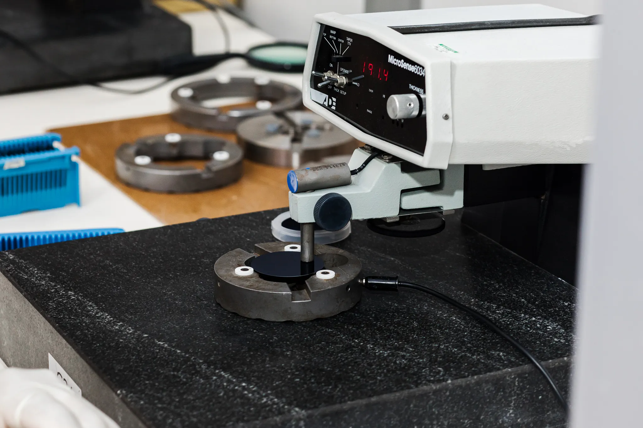
One of the semiconductor industry's most widely used etching techniques is reactive ion etching. Reactive ion etching can remove organic material, which uses ion transfer. The RIE technique is frequently chosen for numerous production processes because ion etching is a dry process in contrast to conventional etchants.
It is, nevertheless, much more versatile than other etching techniques. The etching rate can be managed by increasing the ICP-RIE reactor's power. Sensitive electronics are at risk from plasma because of the process's high temperature. As a result, it's crucial to shield delicate electronic components from extreme heat and ion beams.
A physical dry etchant is used in this procedure. Argon ions with energy between one and three keV are emitted on a surface during the etching process. The wafer is positioned parallel to the ion beam. As a result, the etching process is completely anisotropic, but the selectivity is low because it is impossible to tell one layer from another.
The plasma's oxygen content plays a significant role in determining the etching rate. The effectiveness of the oxidation process may be enhanced by more oxygen in the plasma. Gas flow rate management is necessary for semiconductor devices to avoid excessive etching. However, a higher oxygen level may make the SiC-etched surface less rough.
This method's versatility and flexibility are its key advantages. Users of this kind of etching method can regulate the rate of etching as well as its repeatability, homogeneity, and anisotropy. It is also the quickest and most versatile technique for dry etching.
At Wafer World, our team can provide helpful information about silicon wafers. If you want to learn more about this material, contact our team today!


