July 30, 2025
Shop NowWafer-to-wafer bonding is a potent technique for producing semiconductors that physically unite two wafers to form intricate, multilayered structures. It is crucial in technologies that need miniaturization, 3D stacking, or the integration of different materials or device types. Wafer-to-wafer bonding can involve a variety of materials, from a silicon wafer to a more complex compound substrate.
Although it offers significant performance and scaling advantages, it also requires exact control over alignment, cleanliness, and thermal compatibility to guarantee high yield and dependability. Understanding these factors in detail is crucial to guaranteeing a successful result.
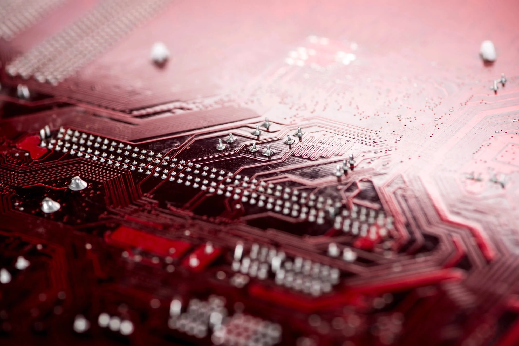
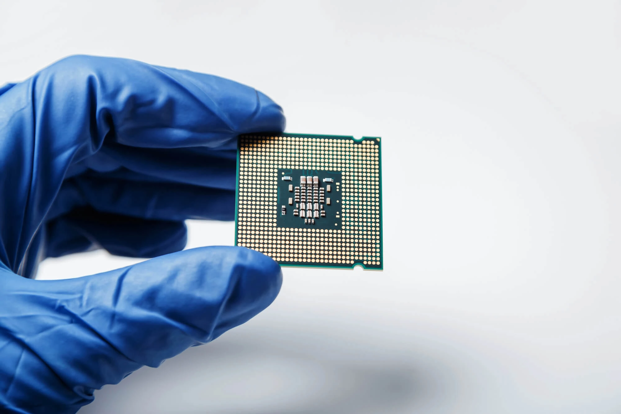
A fabrication process called wafer-to-wafer bonding combines two semiconductor wafers chemically or physically, aligning them precisely at the wafer scale to create a cohesive structure.
This method is frequently employed in producing sophisticated semiconductors, including image sensors, MEMS (micro-electro-mechanical systems), 3D integration, and heterogeneous integration. It involves the following key steps:
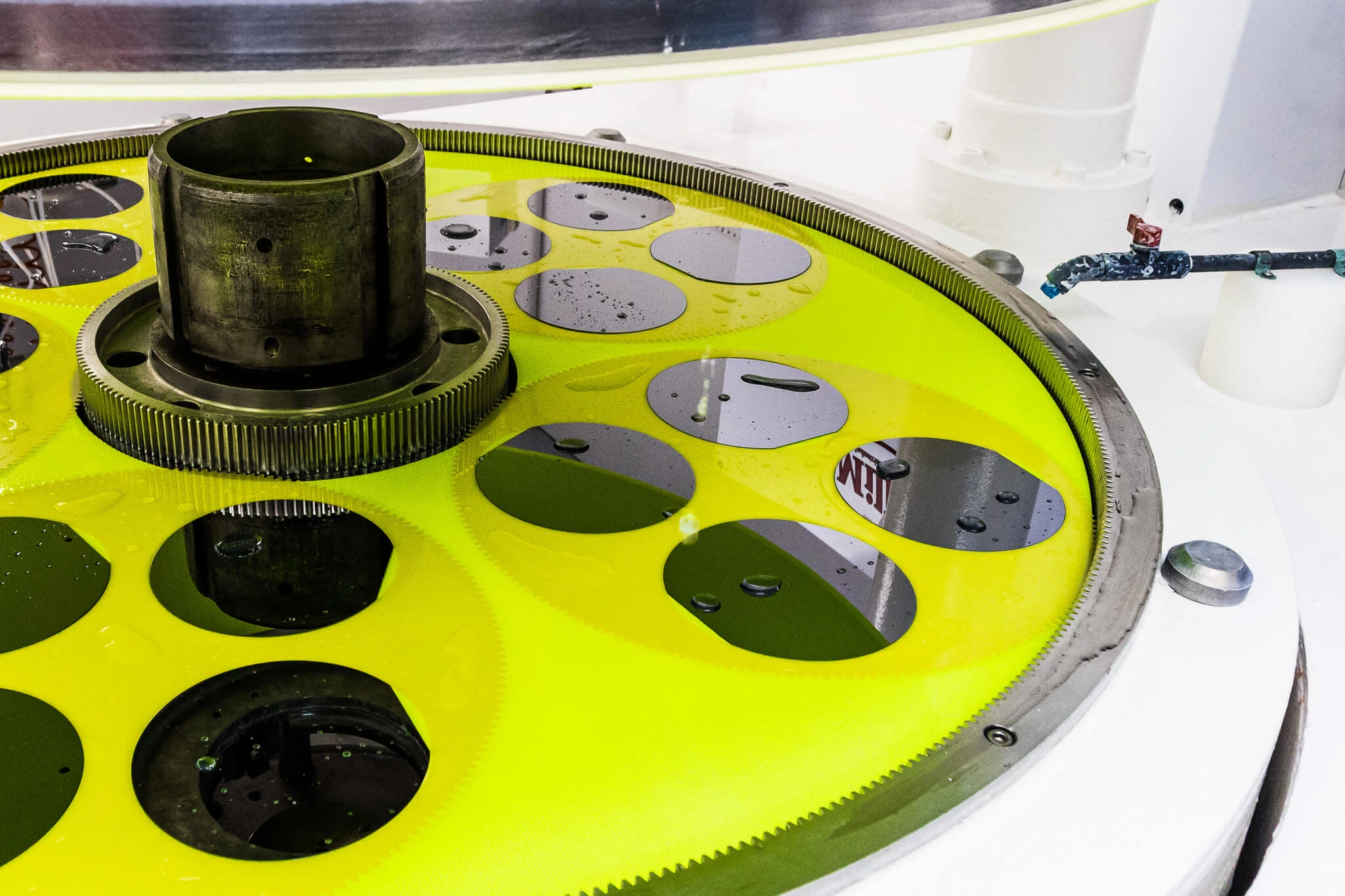
The wafers are cleaned and polished to guarantee smooth, particle-free surfaces. Activation is also necessary for some bonding methods (like plasma treatment) to increase bonding strength.
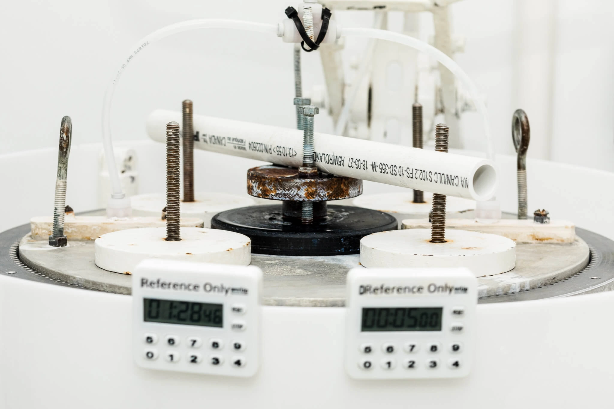
Wafers are precisely aligned using alignment marks to ensure that features (like circuits or microstructures) on both wafers line up accurately.
The wafers are brought into contact under controlled conditions. Depending on the type of bonding, they may adhere immediately at room temperature or require thermal or pressure treatment to strengthen the bond.
Sometimes, after bonding, one of the wafers—typically the handle wafer—is thinned or etched to reveal functional layers or allow for additional integration.
Wafer-to-wafer bonding is a crucial step in the production of sophisticated semiconductors. Some of the complex system architectures achievable through wafer-to-wafer bonding include:
One of the most significant applications of wafer-to-wafer bonding is in 3D integrated circuits.
In 3D ICs, multiple wafers or dies are stacked vertically to form a compact device. This stacking approach reduces interconnect length, improves signal speed, and lowers power consumption.
Wafer bonding is widely used in manufacturing CMOS image sensors, especially those with backside illumination (BSI).
In these devices, a photosensitive wafer is bonded to a readout wafer, exposing the pixel array from the back side, increasing light sensitivity and image quality. This technique is crucial in producing high-resolution cameras for smartphones, medical imaging, automotive systems, and security cameras.
In MEMS fabrication, wafer bonding encapsulates mechanical structures like pressure sensors, accelerometers, or resonators. The bonding process can create sealed cavities that protect sensitive components or enable mechanical movement.
Wafer-to-wafer bonding also enables the integration of MEMS structures directly on top of CMOS wafers, combining sensing and processing on the same chip.
Wafer bonding enables heterogeneous integration, where wafers made of different semiconductor materials—such as silicon, gallium arsenide (GaAs), or indium phosphide (InP)—are bonded together.
This allows the combination of materials with different electronic or optical properties. For instance, bonding a GaAs laser wafer to a silicon photonic wafer enables high-performance optical communication systems without silicon alone.
In power electronics, wafer bonding integrates high-voltage devices with control electronics or bonds thin-film layers onto robust substrates for improved heat dissipation.
Additionally, in biosensors and chemical sensors, bonding techniques seal fluidic channels or isolate sensing regions, making the devices more reliable and durable in harsh environments.
Wafer-to-wafer bonding, especially involving silicon wafers, is a powerful integration method—but it comes with a number of technical challenges that can significantly affect yield, performance, and reliability if not properly addressed.
Some of these include:
For effective bonding, especially in direct (fusion) bonding, the wafer surfaces must be extremely flat and smooth (roughness < 1 nm RMS). Silicon wafers often undergo chemical-mechanical polishing (CMP) to achieve this, but even slight warping or particle contamination can create voids or prevent proper bonding.
Particles (even on the order of nanometers) between wafers can prevent local bonding, leading to void formation or delamination. This is especially problematic for wafer-scale processing, where a single defect can compromise the entire wafer.
Even between two silicon wafers, thermal expansion mismatches can arise if the wafers have different doping levels, materials, or thicknesses. This mismatch becomes more critical when bonding silicon with other materials like glass, III-V compounds, or metals.
For 3D integration and CMOS image sensors, sub-micron or even sub-100 nm alignment between wafers is required. Misalignment can lead to misconnected TSVs, interconnect failure, or optical misregistration.
In some cases, the initial bond formed may not be strong enough for further processing, especially for high-temperature or back-end-of-line (BEOL) operations. Additional annealing may be required, but this introduces thermal stress and can degrade previously formed structures.
Even small variations in wafer thickness or residual stress (from prior processing) can cause bowing or warping, making uniform contact during bonding difficult.
In wafer-to-wafer bonding, one bad die on either wafer ruins both dies at that location. Compared to die-to-wafer bonding (where known-good dies are used), wafer-to-wafer bonding is less forgiving and more yield-sensitive.
Wafer bonding involves sophisticated equipment for cleaning, alignment, bonding, and post-bond annealing. Any variation in process parameters (like pressure, temperature, alignment time) can result in defects.
Wafer-to-wafer bonding is a fundamental technology that makes many of our world's most sophisticated applications possible. From MEMS and heterogeneous integration to 3D memory and high-resolution imaging, this technique pushes the limits of functionality, performance, and miniaturization in electronic devices.
As semiconductor technology advances, wafer bonding will remain essential to creating more intelligent, quicker, and integrated systems. If you’d like to explore these advantages by yourself with a silicon wafer, we can help. Contact Wafer World and learn all about our substrate materials!


