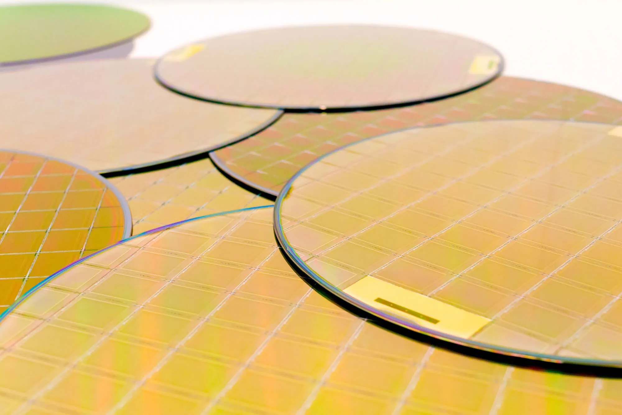
Thin silicon wafers are often ~100–50 μm thick, which significantly increases energy efficiency, power density, and reliability in power conversion solutions for AI data centers, consumer, motor control, and computing applications. Often, the process for manufacturing these ultra-thin wafers starts with the CZ silicon-growth method.

The Czochralski method is used for growing large, high-purity single-crystal silicon ingots. The crystal is pulled slowly from molten silicon to ensure proper atomic arrangement (that is, a monocrystalline structure).
In simple terms, the Czochralski method works by:
It produces ingots typically 300 mm in diameter and up to 1–2 meters long. These are then sliced into the ultra thin wafers used to fabricate integrated circuits and solar cells.
CZ-grown silicon is a substrate that offers high purity, relatively high oxygen content, and mechanical hardness. Once the ingot is developed, wafers are mechanically or chemically thinned to ultra-thin dimensions (e.g., <100 μm), using back grinding, chemical mechanical polishing (CMP), or wet or dry etching.
This results in a semiconductor that’s ideal for applications where space, flexibility, weight, or thermal management are critical, such as 3D ICs, wearable electronics, photovoltaics used in solar cells, and more.
Contact us today if you’d like to learn more about Wafer World's manufacturing methods!


