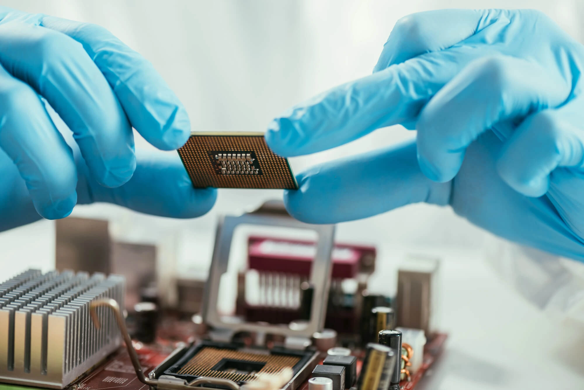
When it comes to semiconductors, precision and consistency are key standard—and in order to achieve that, a double side polish wafer can make the difference.
Double side polish wafers are carefully polished on both sides to create a very smooth and flat surface. This level of precision is crucial for applications that require the highest level of accuracy, and as chip design becomes more intricate, its uses will grow.
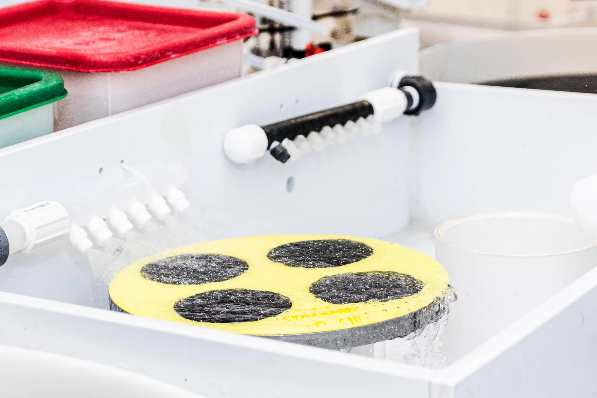
In semiconductor manufacturing, double-side polishing (DSP) is a wafer finishing technique that produces incredibly smooth, flat surfaces on both sides of a silicon wafer.
For many standard applications, single-side polished (SSP) wafers are adequate.
However, DSP wafers are necessary for high-precision, high-performance devices where mechanical symmetry, cleanliness, and surface flatness are crucial. This is the case for:
DSP wafers are frequently needed for power devices like thyristors, high-voltage MOSFETs, and insulated-gate bipolar transistors (IGBTs). These devices are usually made on thicker wafers for mechanical strength because they handle high voltages and large currents.
Double-side polishing enhances wafer parallelism and flatness, which is important for high-temperature processing stages like diffusion and epitaxy. Furthermore, DSP ensures uniformity during die attachment and packaging by reducing bowing and warping in thick wafers.
Such mechanical and thermal stability is essential for devices such as IGBTs in power grids, industrial motor drives, and electric vehicles.
DSP is a standard requirement for producing SOI wafers, which are utilized in radiation-hardened devices, RF circuits, and high-performance digital and analog integrated circuits.
The SOI structure consists of a thin silicon layer supported by a silicon handle wafer on top of an insulating layer, typically silicon dioxide. To achieve such a layered structure, two wafers must be precisely bonded, and double-side polished surfaces are essential for this process.
Polishing both sides ensures excellent bonding quality and lowers the possibility of voids or defects, making it possible to create cutting-edge devices with faster speeds, fewer parasitics, and lower power consumption.
MEMS devices combine electronics, sensors, actuators, and mechanical components onto a single silicon substrate. Examples include pressure sensors, microphones, gyroscopes, and accelerometers.
These devices frequently need the wafer to be precisely etched on both sides to create moving parts or cavities—enter the DSP wafer.
Double side polishing provides the necessary flatness and thickness uniformity for accurate front-and-back alignment during deep reactive ion etching (DRIE) and other lithographic processes. DSP once more guarantees correct alignment and bonding strength during wafer bonding, another step in MEMS manufacturing.
DSP wafers are occasionally needed for optoelectronic devices such as photodiodes, image sensors (such as CMOS image sensors), and light-emitting diodes (LEDs).
These devices are sensitive to surface contamination and structural irregularities. Double-sided polished wafers increase light transmission and sensor precision by lowering contamination, flaws, and scattering. For back-illuminated sensors that receive light from the wafer's backside, a smooth, clean rear surface is crucial to optimizing optical efficiency.
Even though SSP wafers are used to fabricate many common logic and memory integrated circuits, advanced nodes, particularly those that use FinFET or gate-all-around (GAA) transistor architectures, might need DSP substrates for certain fabrication processes.
For example, wafers undergoing wafer-to-wafer bonding, backside power delivery integration, or advanced stacking (3D ICs) benefit from having both sides polished. DSP minimizes defects and topographical variations that can interfere with high-resolution lithography and bonding processes.
Through-Silicon Via (TSV) technology enables vertical electrical connections through a silicon wafer, allowing for high-density 3D integration of semiconductor devices. TSVs are widely used in advanced packaging, including 3D memory stacks, system-in-package (SiP) designs, and heterogeneous integration.
TSV processes involve etching and metallizing features throughout the wafer. DSP wafers are crucial for uniform etching and alignment. The double-polished finish ensures minimal wafer bow, which is critical for deep etching and uniform dielectric and metal deposition throughout the wafer thickness.
Additionally, DSP wafers improve the quality of wafer bonding and thinning processes, both of which are common in TSV integration flows.
While silicon is the most common wafer material, double-side polishing is also applied to compound semiconductor substrates like gallium arsenide (GaAs), silicon carbide (SiC), and gallium nitride (GaN).
These materials are used in RF devices, high-power transistors, and LEDs. SiC, for instance, is used for high-efficiency power devices, and DSP is often needed due to the material's high thermal conductivity and hardness. Flatness and minimal subsurface damage are critical for device yield and performance, especially when thinning wafers or using double-sided processing.
8. Wafer-Level Packaging and 3D Integration
In wafer-level packaging (WLP) and 3D IC integration, devices are stacked and interconnected vertically, requiring ultra-flat wafers to ensure strong and reliable wafer-to-wafer bonds.
Double-sided polished wafers ensure the mechanical integrity for through-silicon vias (TSVs), redistribution layers (RDLs), and other fine-pitch interconnects. This is increasingly important in smartphones, wearables, and high-performance computing, where space and performance constraints demand vertical integration.
In addition to their importance in commercial semiconductor manufacturing, double-side polished (DSP) wafers play a crucial role in research and development (R&D) across universities, government labs, and corporate research centers.
DSP wafers are often a foundational platform for experimentation and innovation, whether used to develop next-generation transistors, prototype micro- and nanoscale devices, or test novel materials.
Researchers experimenting with wafer bonding techniques—such as direct, anodic, or fusion—rely heavily on DSP wafers. The success of these bonding methods depends on extremely smooth and clean surfaces to create void-free, strong bonds. Any particles, scratches, or surface bowing can compromise the bond and invalidate experimental results.
DSP wafers are also often used in early-stage prototyping of emerging technologies.
Double side polish wafers are essential in several high-end semiconductor applications. Devices requiring extreme flatness, mechanical stability, or precision alignment—such as power electronics, MEMS, SOI-based circuits, optoelectronics, and 3D ICs—all depend on DSP wafers to meet strict fabrication requirements.
Additionally, double side polish wafers are gaining a unique place in investigation and research for various types of technologies. If that’s your case, here at Wafer World, we aim to maintain an available stock of our products to ensure the supply for our clients. If you need one for your project, contact us today! We’ll do everything we can to get it to you as soon as possible.


