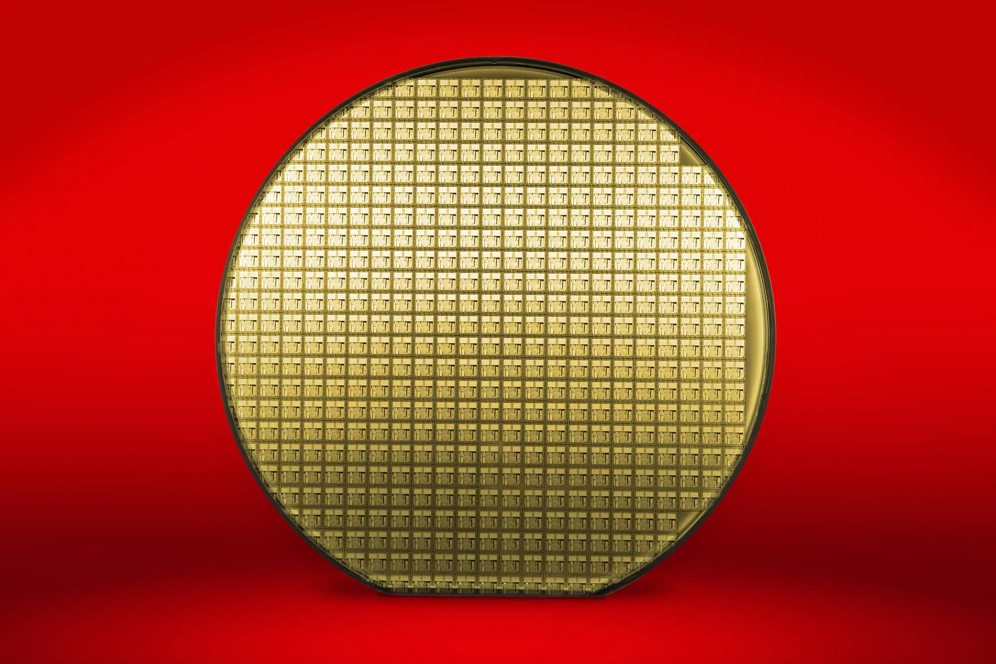
In the world of semiconductor manufacturing, precision and consistency are paramount. One critical component of this intricate process is the silicon wafer, a thin, flat disc of crystalline silicon serving as the foundation for integrated circuits and microchips. While silicon wafers come in various forms, the double-side polish wafer stands out for its exceptional quality and applications.

Double-side polished wafers are silicon substrates that have undergone a meticulous polishing process on both sides to achieve an extremely flat and smooth surface. This level of precision is essential for applications that demand the utmost accuracy, such as in manufacturing high-performance electronic devices.
Double-side polishing ensures uniform thickness and smoothness across the entire wafer. This consistency is vital for creating integrated circuits with minimal defects and consistent performance.
The high-quality surface of double-side polished wafers reduces the likelihood of defects during semiconductor fabrication. This leads to higher yields and cost-effective production.
These wafers are used in applications requiring exceptional optical clarity, such as sensors, optical lenses, and photovoltaic devices. The polished surfaces minimize scattering and distortion, making them ideal for optical components.
Double-side polished wafers offer improved bonding properties, making them suitable for applications like wafer bonding, which is critical for creating 3D integrated circuits and MEMS (Micro-Electro-Mechanical Systems).
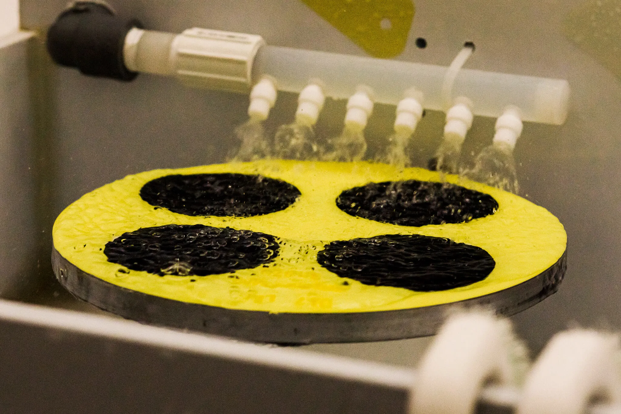
The ultra-smooth surfaces of these wafers are less prone to contamination, ensuring a cleaner production environment and better semiconductor quality.
Double-side polished wafers find applications in a wide range of industries, including semiconductor manufacturing, microelectronics, MEMS fabrication, and photonics. Their exceptional quality and precision make them indispensable for producing advanced electronic devices and optical components.
Double-side polished wafers represent a pinnacle of precision in semiconductor manufacturing. Their uniformity, quality, and versatility make them an essential substrate for cutting-edge technology, ensuring the development of faster, more efficient, and higher-performance electronic devices in our increasingly connected world.
With Wafer World, you are at the forefront of taking advantage of double-side polish wafers! Call us today!


