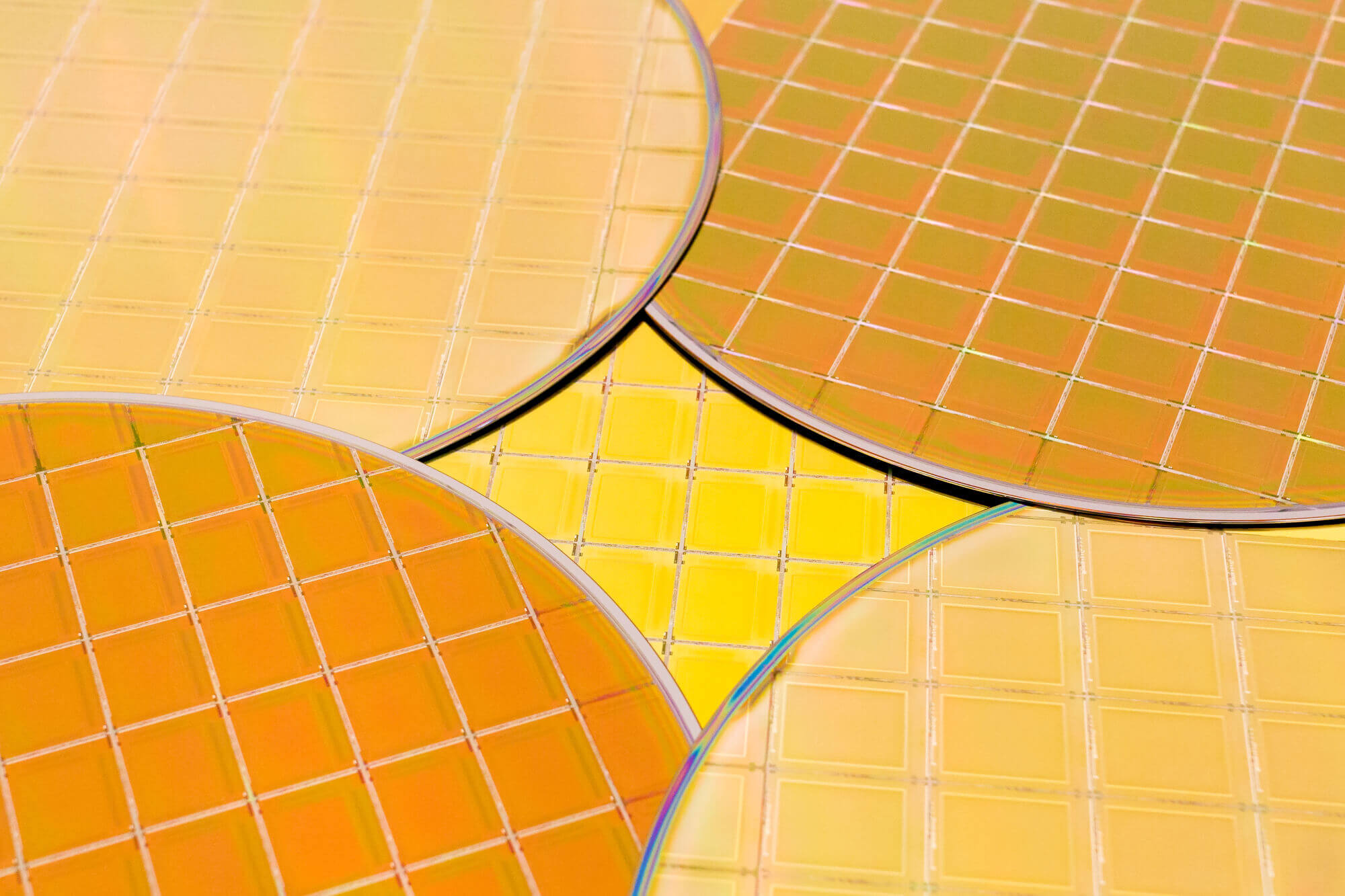
In the realm of semiconductor manufacturing, precision reigns supreme. The quality of silicon wafers, the bedrock of contemporary electronics, profoundly influences the efficacy and durability of semiconductor devices from silicon wafer suppliers. Surface roughness, flatness, and polishing techniques hold paramount importance among the myriad factors shaping wafer quality.
In this comprehensive exploration, we uncover the intricacies of optimizing wafer surface quality, shedding light on techniques and strategies to achieve excellence.
Strategies for Enhancing Wafer Surface Quality
Surface Roughness: The Pursuit of Smoothness
Surface roughness, measured in nanometers, delineates the irregularities on a silicon wafer's surface. Minimizing roughness is critical as it directly impacts the performance and yield of semiconductor devices. Elevated roughness levels can lead to defects, reduced electrical conductivity, and compromised device reliability.
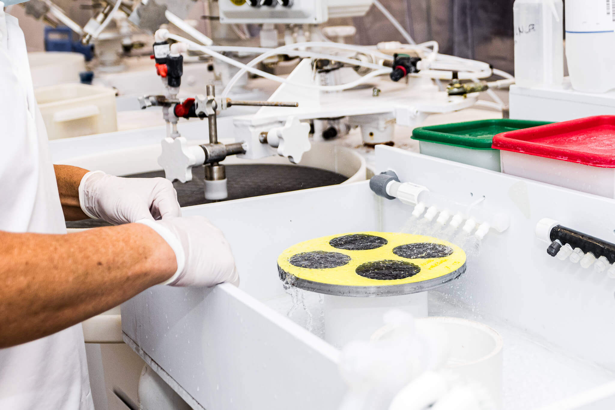
Manufacturers deploy advanced polishing techniques such as chemical-mechanical polishing (CMP) and mechanical grinding to attain the desired smoothness. CMP involves the synergistic action of chemical etchants and mechanical abrasion to effectively eliminate surface irregularities.
Mechanical grinding, conversely, utilizes precision machinery to systematically flatten the wafer surface. Additionally, innovative approaches like plasma-enhanced chemical vapor deposition (PECVD) coatings are employed to refine surface roughness further.
Flatness: The Pursuit of Uniformity
Flatness, the measure of a wafer's surface planarity, is indispensable for ensuring consistent device performance across the wafer. Any deviation from flatness can result in irregular device characteristics, impacting functionality and yield. Therefore, achieving optimal flatness is paramount in semiconductor manufacturing.
Advanced metrology techniques, including interferometry and atomic force microscopy (AFM), facilitate precise characterization of wafer flatness. Additionally, manufacturers utilize sophisticated polishing and lapping processes to eradicate surface undulations. These techniques transform irregular surfaces into epitomes of flatness by applying controlled pressure and abrasive slurries.
Polishing Techniques: Precision in Action
Polishing techniques are pivotal in refining silicon wafer surfaces to meet stringent quality standards. Various methods, each tailored to specific requirements, impart the desired smoothness and flatness.
Chemical-Mechanical Polishing (CMP): CMP, a cornerstone of wafer manufacturing, involves the simultaneous action of chemical etchants and mechanical abrasion. This synergistic approach ensures precise material removal, producing ultra-smooth surfaces with minimal defects.
Mechanical Grinding: Mechanical grinding employs precision machinery to remove surface irregularities and achieve the desired flatness. Manufacturers can tailor the grinding process to meet exact specifications through the controlled application of abrasive pads and slurries.
Polishing Pads and Abrasives: The selection of polishing pads and abrasives is critical in determining the efficacy of polishing processes. Advanced materials such as polyurethane-based pads and nanoscale abrasives enable unparalleled precision and control, ensuring superior surface quality.
Diamond Polishing: Diamond polishing harnesses the exceptional hardness of diamond abrasives to offer unmatched precision and uniformity. By leveraging the unique properties of diamonds, manufacturers can achieve ultra-smooth surfaces with outstanding flatness and minimal surface defects.
Chemical Treatments: Chemical treatments, including etching and surface modification processes, complement mechanical polishing techniques. These treatments facilitate the removal of surface contaminants and defects, enhancing surface smoothness and purity.
In-Situ Monitoring: Real-time monitoring techniques, such as optical profilometry and laser interferometry, enable in-situ assessment of polishing progress. Manufacturers can optimize process parameters by continuously monitoring surface characteristics to achieve the desired surface quality.
The Synergy of Techniques: A Holistic Approach to Wafer Surface Optimization
In the pursuit of perfection, semiconductor manufacturers adopt a holistic approach that integrates multiple techniques to optimize wafer surface quality. By synergistically combining polishing, grinding, and chemical treatments, manufacturers can achieve surfaces that meet the exacting demands of modern semiconductor devices.
Key strategies for optimizing wafer surface quality include:
Process Integration: Seamlessly integrating polishing, grinding, and chemical treatments into a cohesive manufacturing workflow ensures consistent and reproducible results.
Parameter Optimization: Fine-tuning process parameters such as pressure, speed, and abrasive concentration is essential for achieving the desired surface quality.
Material Selection: Careful selection of polishing pads, abrasives, and chemical treatments is crucial for meeting specific performance requirements and minimizing surface defects.
Metrology and Quality Control: Rigorous metrology and quality control protocols, including real-time monitoring and post-processing characterization, ensure adherence to stringent quality standards.
By embracing these strategies, semiconductor manufacturers can elevate wafer surface quality to new heights, enabling the realization of next-generation electronic devices with unparalleled performance and reliability.
Expanding on Surface Quality Optimization
In addition to the core elements of surface roughness, flatness, and polishing techniques, there are several other aspects of wafer surface quality optimization worth exploring:
Surface Cleanliness: Ensuring the cleanliness of wafer surfaces is vital for preventing contamination and defects. Advanced cleaning methods, such as megasonic and ozone cleaning, are employed to remove residual particles and contaminants.
Surface Defect Reduction: Minimizing surface defects, such as scratches, pits, and particles, enhances wafer quality. Techniques like defect inspection and mitigation and defect engineering are utilized to identify and eliminate defects during the manufacturing process.
Surface Functionalization: Functionalizing wafer surfaces with specific coatings or treatments can enhance performance and functionality. Surface modification techniques, including self-assembled monolayers (SAMs) and plasma treatments, are employed to tailor surface properties for specific applications.
Surface Texture Control: Controlling surface texture, roughness, and flatness can impact device performance and functionality. Surface texturing techniques, such as laser patterning and microstructuring, are utilized to impart desired surface features for improved device performance.
Surface Contouring: Contouring the wafer surface to match specific device geometries and requirements is essential for certain applications, such as MEMS (microelectromechanical systems) and sensors. Advanced machining techniques, including laser ablation and chemical etching, are employed to precisely contour the wafer surface to meet design specifications.
Surface Coating Deposition: Depositing thin films or coatings onto wafer surfaces can enhance functionality, protection, and compatibility with subsequent processing steps. Techniques such as physical vapor deposition (PVD) and chemical vapor deposition (CVD) are utilized to deposit thin films of metals, oxides, or polymers onto wafer surfaces with precise control over thickness and uniformity.
By addressing these additional aspects of surface quality optimization, semiconductor manufacturers can further enhance wafer quality and drive innovation in electronic device manufacturing.
Order from a Trusted Silicon Wafer Supplier Today!
Optimizing wafer surface quality is a multifaceted endeavor that demands precision, expertise, and innovation. Through the synergistic application of polishing techniques, manufacturers can achieve surfaces that meet the stringent demands of modern semiconductor devices. Semiconductor manufacturers can unlock new possibilities in device performance and reliability by embracing a holistic approach that integrates polishing, grinding, chemical treatments, and other surface quality optimization strategies.
As Wafer World technology continues to advance, the pursuit of perfection in wafer surface quality remains paramount, driving innovation and advancement in the semiconductor industry. Order today!