Did you know that silicon wafers are produced in two ways? While the Czochralski method grows single crystals of silicon semiconductors, the float zone method melts a high-purity polycrystalline rod and monocrystalline seed crystals under a vacuum. Compared to the thin silicon wafer produced via the Czochralski method, the float zone wafers have proven themselves to be a high-quality alternative.
Polish chemist named Jan Czorchralski accidentally discovered this method in 1916. Instead of dipping his pen into his inkwell, Czorchralski dipped it into a container of molten tin. Although he was able to pull his pen out right away, he noticed a thin strand of solidified metal hanging from its nib. Later, he was able to verify that the crystallized metal is a single crystal with no grain boundaries.Today, single crystals of semiconductors including silicon, gallium arsenide, and germanium, along with various metals, salts, and synthetic gemstones, are grown through the Czorchralski method. Aside from producing semiconductors, this method is also used to create large cylindrical ingots or boules.The process starts with melting high-purity silicon in a crucible. Next, a seed crystal is mounted on a rod and is dipped into the molten material. As the rod is being simultaneously pulled upward and rotated at a constant rate and speed under a precisely controlled temperature, it extracts a single crystal, cylindrical ingot.

Henry Theurer, a Bell Labs chemist, discovered the float zone method, which uses the zone-melting principle taking place under a vacuum. Unlike the Czorchralski method, the float zone method grows single crystals without the use of a crucible. Instead, the molten zone is maintained between two solid vertical rods via its own surface tension.

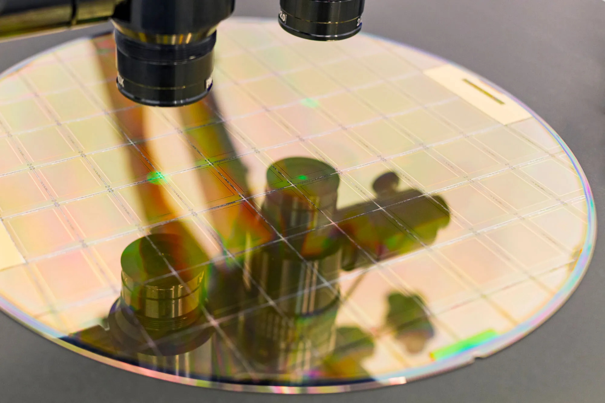
Float zone wafers are made of high-purity crystals that were produced through the float zone process. Due to their extremely low levels of light impurities, they tend to restrain micro-defects and exhibit enhanced mechanical strength.For this reason, most manufacturers prefer to use float zone wafers for their projects instead of the standard wafers grown through the Czochralski method that have moderate levels of light impurities. If you’re planning to use float zone wafers for your next project, contact Wafer World today.


