
If you've mostly worked with silicon, a germanium wafer may feel like a "shortcut material": faster carrier transport, strong near-IR usefulness, and device behaviors that emerge clearly even with minor doping or temperature changes. That's the advantage—and the reason specifications are more important than a generic "Ge wafer" line item.
Nevertheless, understanding germanium’s electrical properties and what distinguishes them is crucial to making the most out of those properties in real-world device decisions.

Germanium’s electrical personality comes from a specific combination of fundamentals:
Given these factors, germanium is commonly considered for high-speed electronics and near-IR photonics. However, it also explains why this material can be famously unforgiving if you underspecify the wafer. So, how can you optimize germanium’s electrical properties?
Germanium’s room-temperature bandgap is listed at ~0.661 eV. That narrow gap is a big part of why Ge can be attractive for optoelectronics and high-speed transport, but it also means:
If your success metric is low dark current or low off-state power, you’ll typically need to treat leakage as a first-class design constraint (not a late-stage “we’ll tweak it” issue).
For high-purity/weakly doped Ge, references commonly show electron mobility up to ~3900 cm²/V·s and hole mobility up to ~1900 cm²/V·s at 300 K.
So, for a given geometry, you can often get higher transconductance or faster response than you’d expect from silicon assumptions.
Nevertheless, germanium’s mobility is doping-dependent—if you push very heavy doping to hit ultra-low resistivity, mobility will drop and your “speed” advantage can shrink.
Germanium possesses an intrinsic carrier concentration of ~2.0×10¹³ cm⁻³ and an intrinsic resistivity of ~46 Ω·cm.
For that reason, Ge devices can be more sensitive to temperature drift in leakage/noise.
This is also one reason high-purity germanium is used in radiation detectors—but those systems often lean on cooling to suppress thermal carriers because Ge’s bandgap is relatively low.
Germanium’s dielectric constant, ~16.2 (300 K), is notably higher than silicon’s. In plain terms: fields “see” Ge differently.
Junction capacitance and device parasitics can be larger than a silicon-based intuition would suggest in high-speed designs, which can affect bandwidth unless you manage geometry carefully.
A commonly cited order-of-magnitude value for Ge is a breakdown field ≈of 10⁵ V/cm. That doesn’t mean “Ge breaks easily” in every structure—it means your layout and doping profiles should respect field crowding, especially near edges and interfaces.
Even though this guide is “electrical,” heat transport changes electrical outcomes through mobility, leakage, and lifetime effects. Ge’s thermal conductivity lies at 0.58 W·cm⁻¹·°C⁻¹ (≈58 W/m·K).
If your application has high power density or a high duty cycle, plan for thermal design early—especially because Ge’s narrow bandgap makes temperature-related electrical drift more pronounced.
Generally speaking, understanding a material’s electrical properties before incorporating it is important—but in these areas, it becomes critical for success:
Germanium is widely used for photodetectors around the optical communications bands (1.3 µm and 1.55 µm), particularly when integrated onto silicon platforms. Here, germanium’s band structure supports strong absorption in that region, enabling practical on-chip detection.
Ge’s lattice constant is commonly listed as ~5.658 Å. That puts it very close to GaAs (often cited as a motivation for III–V integration strategies), and researchers note Ge can serve as a buffer layer for III–V growth approaches.
Not always. Ge has much higher mobilities, but its narrower bandgap and higher intrinsic carriers may increase leakage sensitivity. "Better" depends on what you're trying to achieve.
A narrower bandgap (~0.661 eV) and high intrinsic carrier concentration (~2.0×10¹³ cm⁻³) increase thermal generation and can amplify leakage mechanisms under high field.
Often, the best way to streamline procurement processes (and thus ensure their success) is clear communication. If you want fewer back-and-forth emails and fewer “wrong wafer” surprises, we recommend defining and expressing these 6 factors during your inquiry:

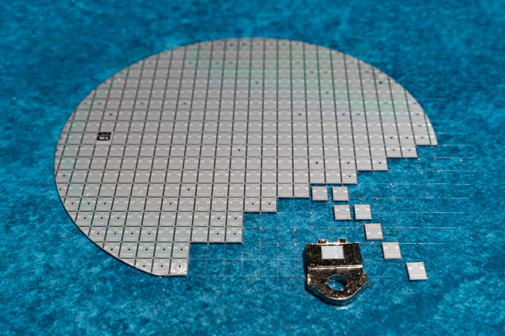
Wafer World supplies germanium wafers in the R&D-to-pilot range and provides reclaim services. If you tell us your electrical target (speed, leakage, detector band, junction behavior), we'll help you translate it into a wafer specification you can buy and quote.
Reach out and let's work together to make your project a reality!


