
Patterned wafers are no longer a specialized tool for advanced semiconductor laboratories. They have become indispensable in process development, metrology, calibration, MEMS, photonics, and device validation, helping engineers reduce risk, shorten development cycles, and manage manufacturing costs—making them crucial to consider before you buy a silicon wafer.
If you intend to use silicon wafers for R&D, pilot production, or tool qualification, understanding patterned wafers—and how to specify them correctly—can mean the difference between dependable results and costly rework.
This guide explains what patterned wafers are, why they are important, how they are manufactured, and what to look for when ordering one.

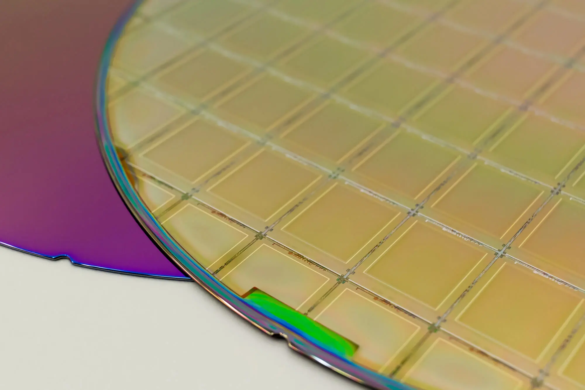
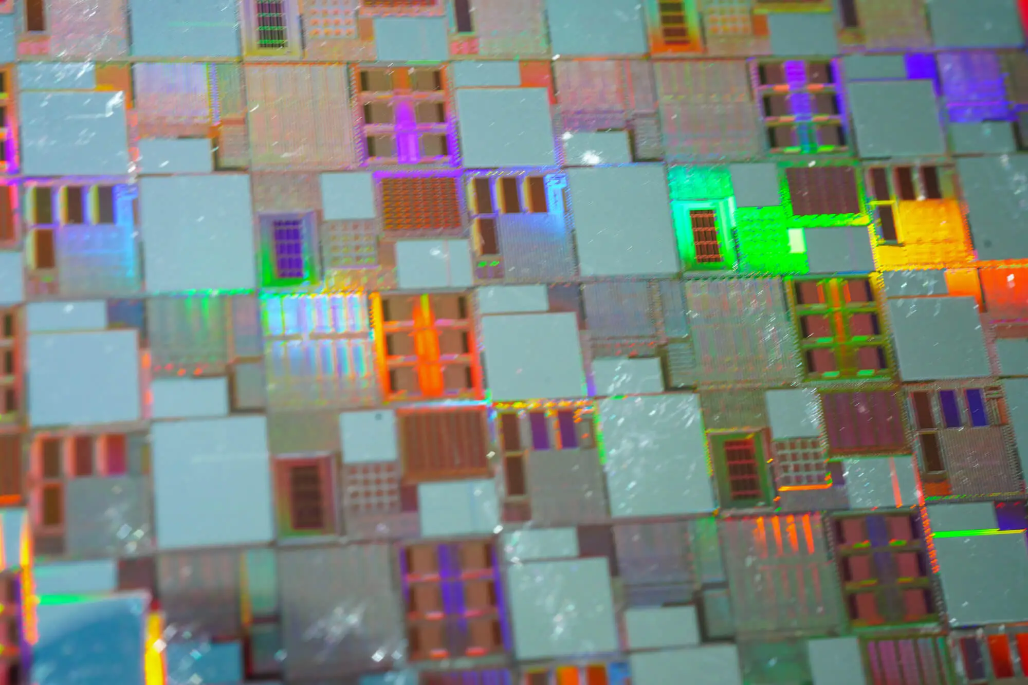
A patterned wafer is a silicon (or compound semiconductor) wafer with intentionally created surface features created through lithography and etching processes. These features can include lines, grids, dots, alignment marks, test structures, or complex device-like geometries.
Unlike blank or prime wafers, patterned wafers are engineered to interact with process tools, measurement systems, or inspection equipment, making them indispensable for:
Patterned wafers act as a controlled reference point in semiconductor manufacturing. Because the geometry, spacing, and material properties are known in advance, engineers can use them to isolate process variables with high precision.
Some of the main reasons why patterned wafers matter include:
According to SEMI, early-stage test wafers significantly reduce downstream manufacturing risk
Patterned wafers can vary widely depending on application, substrate, and feature geometry. Choosing the right type depends on what you need to measure, calibrate, or validate, as each pattern is designed to isolate specific process variables.
Used for critical dimension (CD) measurements, etch profiling, and lithography optimization. These patterns allow engineers to evaluate linewidth uniformity, sidewall angle, and process bias, making them essential for fine-tuning photolithography and etching steps.
Ideal for overlay accuracy, alignment calibration, and stepper performance testing. The repetitive and evenly spaced geometry enables precise measurement of placement error, distortion, and tool drift across the wafer surface.
Include resistors, capacitors, van der Pauw structures, or transistors for electrical testing. These structures are designed to translate physical process variations into measurable electrical parameters, supporting process development, monitoring, and fault isolation.
Used to validate tool alignment across multi-layer processes. By providing clearly defined reference marks, these patterns ensure accurate layer-to-layer registration, which is critical for advanced nodes and multi-step fabrication flows.
Patterned wafer fabrication follows many of the same steps used in device manufacturing, but with tighter emphasis on dimensional accuracy and repeatability.
Most patterned wafers are produced on silicon substrates, though SiC, GaAs, and sapphire are also common. Orientation, resistivity, and thickness must be selected upfront.
Photoresist is applied and exposed using a photomask to define the pattern geometry.
Patterns are transferred onto the wafer using wet or dry etching or thin-film deposition.
Final inspection ensures CD tolerance, pattern fidelity, and surface quality.
Patterned wafers are used across nearly every advanced technology sector. They provide a controlled, repeatable platform for validating processes, tools, and designs before full-scale production.
Engineers use patterned wafers to fine-tune lithography, etch depth, and deposition uniformity before committing to device wafers. This reduces risk by allowing early detection of process variability, defects, and yield-impacting issues in a cost-effective development phase.
Patterned wafers are critical for validating measurement tools such as AFMs, CD-SEM systems, and optical profilers. Known feature geometries enable traceable calibration, tool matching, and long-term measurement stability across fabs and equipment platforms.
MEMS devices rely on highly repeatable structures, making patterned wafers essential for process verification. They allow manufacturers to verify mechanical dimensions, release steps, and functional consistency before producing fragile or high-value sensor devices.
Waveguides, gratings, and alignment structures require precise pattern control to achieve optimal optical performance. Patterned wafers help validate critical optical parameters such as coupling efficiency, propagation loss, and alignment tolerance during fabrication.
Besides all of the advantages mentioned, patterned wafers are often chosen because they provide:
If you’re planning to buy silicon wafers with custom patterning, these specifications matter more than most buyers realize:
Patterned wafers are at the intersection of precision, risk reduction, and cost control. Whether you're testing new equipment, optimizing a process, or validating metrology tools, they provide the controlled environment engineers require to make informed decisions.
If your next step is to purchase silicon wafers, selecting the right patterned wafer—built to your exact specifications—can save months of development time and avoid costly downstream errors. At Wafer World, we can help. Reach out, and let’s work together to figure out the ideal material for your project.


