One of the most fascinating aspects of semiconductors is that they come in all shapes and sizes. Because semiconductors are key components of most technologies, the variability in application means that different materials are better suited for certain tasks than others. Historically, silicon has been the most common material used in semiconductor manufacturing, but technological advancements lead to more demanding applications. More demanding uses mean that sometimes silicon is not the optimal choice for certain needs. This is especially true when it comes to photodetectors. Although silicon continues to be the most widely used material in these devices, the germanium wafer is better equipped for the job. Are we on the verge of seeing a major shift in how photodetectors are made? Let’s take a closer look at germanium and get a sense of why this element might soon be the standard for photodetectors.
Germanium is a chemical element metalloid, meaning it has the properties of both metals and nonmetals. It falls right between silicon and tin on the periodic table of elements and has similar semiconducting properties as silicon. For many years after its discovery, germanium did not yield any significant value until its semiconducting properties were discovered in 1945.
One of the most notable aspects of germanium’s history was its discovery. In 1871, Russian chemist, inventor, and creator of the periodic table of elements, Dmitry Mendeleev, predicted the existence of germanium. The element would not be discovered for another 15 years, but its discovery in 1886 validated the periodic table and helped cement its importance in the scientific community.
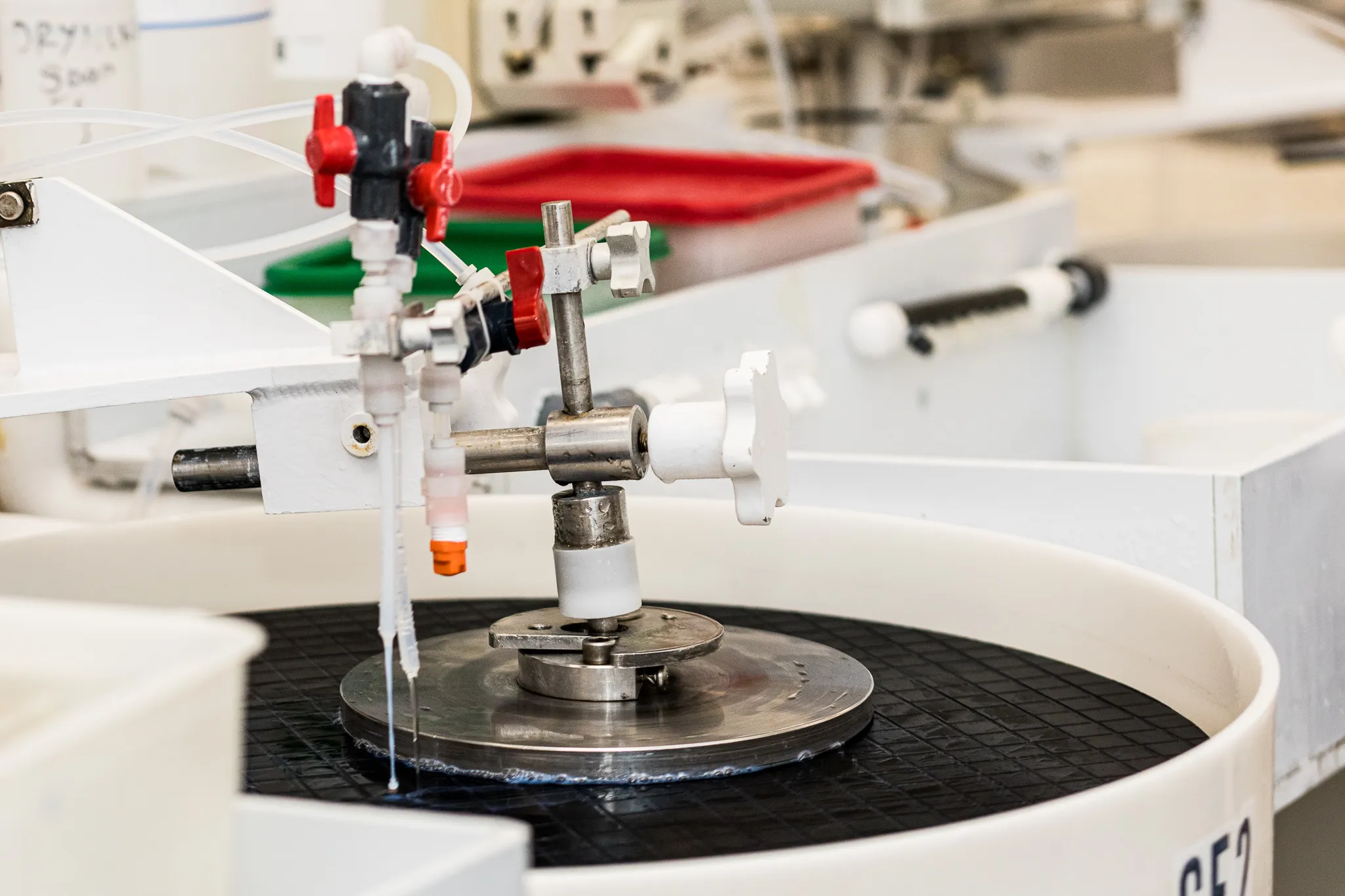
Germanium wafers are one of the most effective semiconductors in the market. Germanium has a similar structure as silicon, but it requires less energy than silicon to create the electron-hole pairs that help transfer electric currents between integrated circuits. The biggest downside to germanium wafers is that they have a small bandgap energy threshold; this means that for high-intensity applications, detectors made from germanium need to be operated at cryogenic temperatures.

Also called photosensors, photodetectors are devices that can register light or similar electromagnetic radiations. Essentially, any device used for registering photons above the frequency of radio waves can be classified as photodetectors.
You might not know it, but photodetectors are everywhere around you. From applications as mundane as the laser sensors that trigger automatic doors at supermarkets to crucial components in giant astronomical arrays used to detect radiation beyond our atmosphere. These devices can be found in a wide range of household and industrial settings, including:
Photodetectors are at the heart of many advanced technologies, and germanium wafers are at the heart of some of the most advanced photodetectors.
As we mentioned, silicon is still the most widely used material for semiconductor manufacturing, and there are a lot of good reasons for that. For starters, silicon is the second most common element on Earth. It’s so abundant, in fact, that it can be found in the sand across the world. Silicon’s abundance and ease of manufacturing have made it an economically efficient option. But that’s not the only reason why silicon remains king. It might seem obvious, but we have created a massive industry around silicon. Factories are optimized to produce silicon wafers, so to trigger an industry shift to a new material could cause enormous, unforeseen expenses that manufacturers are unwilling to front.
There are obvious and subtle reasons for germanium wafers potentially becoming the new standard for photodetector technology:
The sensitivity of a semiconductor refers to how easily it can detect and transfer gamma-radiation. This vector is especially important for photodetectors because their entire job is detecting electric currents. Silicon, although offering a good electron transfer speed, ultimately demonstrates a much lower sensitivity than germanium wafers.
Germanium is already used as the preferred material when making particularly sensitive photodetectors. These include laser rangefinders, LIDAR, quantum optics, and night vision devices.
It would not be hard to adapt the existing manufacturing infrastructure to accommodate large-scale germanium wafer production. Even though most semiconductor manufacturing revolves around silicon, germanium is chemically similar enough to not require a major overhaul of existing equipment.
Although germanium is a more effective semiconductor for photodetection applications than silicon, it doesn’t mean it is the best one. Indium gallium arsenide (GaAs), for example, boasts a higher electron speed and comparable sensitivity. The problem is that those alternatives tend to be prohibitively expensive for large-scale production. Germanium is not only better suited for these applications, but it’s also comparatively inexpensive.
Technology is moving at a break-neck pace, and we can project a higher demand for photodetectors, especially in facilitating high-speed energy. In fact, the most important determining factor in the performance of fiber optic communication performance is the quality of the photodetectors that capture incoming information.
Well, currently, 3.5 billion people out of 7.7 billion have access to the internet. Fewer have access to high-speed internet. But as we become more reliant on the web, access to this resource will become a fundamental necessity for everyone. Experts estimate that by 2069, everyone on Earth will have access to the internet. With more people getting online and more nations depending on their access, we can safely assume that fiberoptic technology will be not just a commodity, but also a matter of national security. Thanks to germanium's unique properties, ease of manufacturing, and superior performance in photodetection as compared to silicon, the element is positioned to become the premier semiconducting material in photodetectors. This change might not come right away as silicon is still the most cost-effective option for “common” uses. However, silicon does have its limitations and germanium wafers can be an effective substitute.

Wafer World is your premier resource for semiconductor wafers of nearly every variety. We are here to educate and provide the highest quality products in the industry. Get in touch with us today to request a quote or learn more about our company!


