.webp)
Indium phosphide wafers are one of the critical components of high-power and high-frequency electronics that make up our intelligent devices' different components. With this device, it's no surprise that you can see them in most appliances we use daily. If you're interested in learning more about InP reclaim wafers, here are some typical applications in the different sectors today.
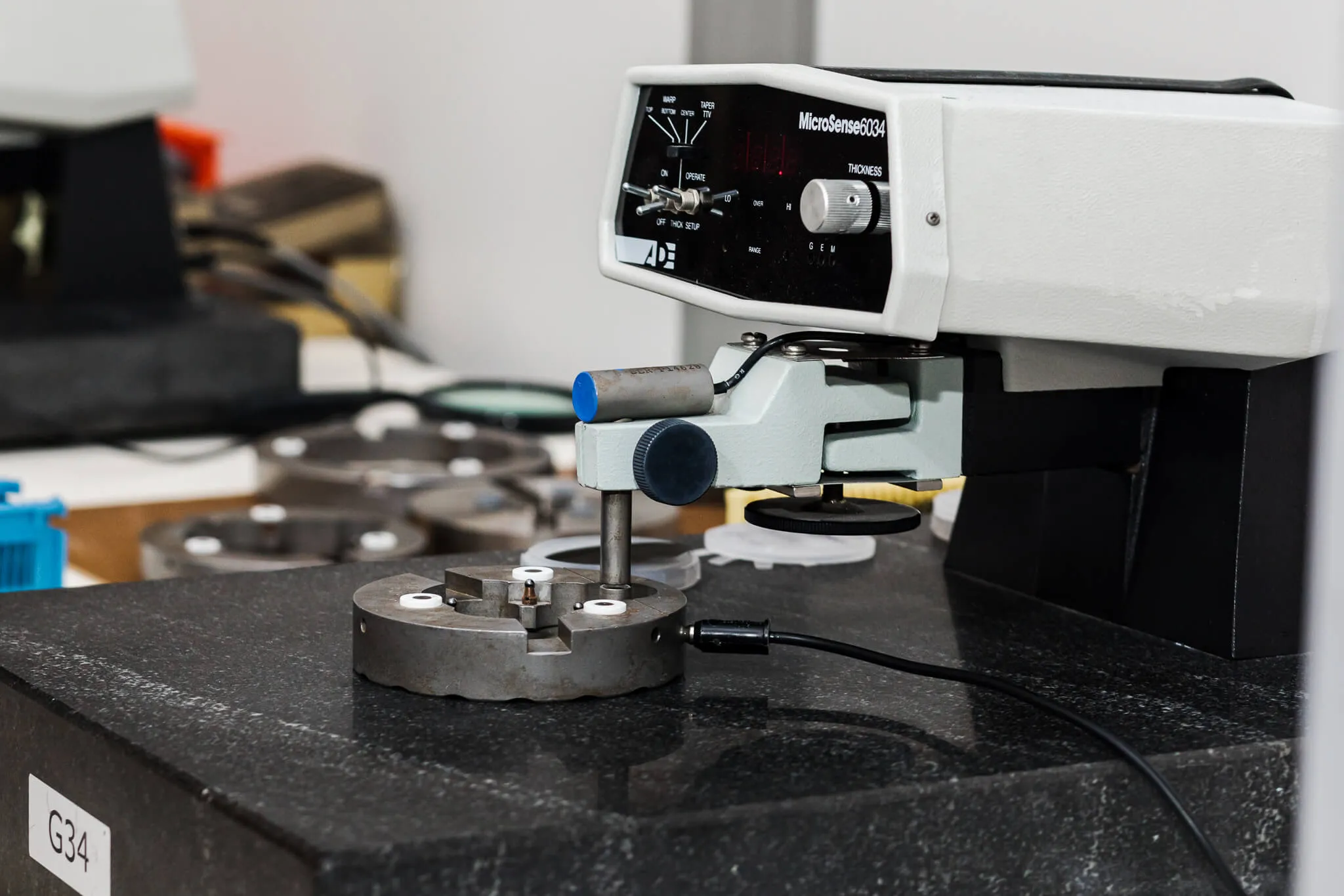
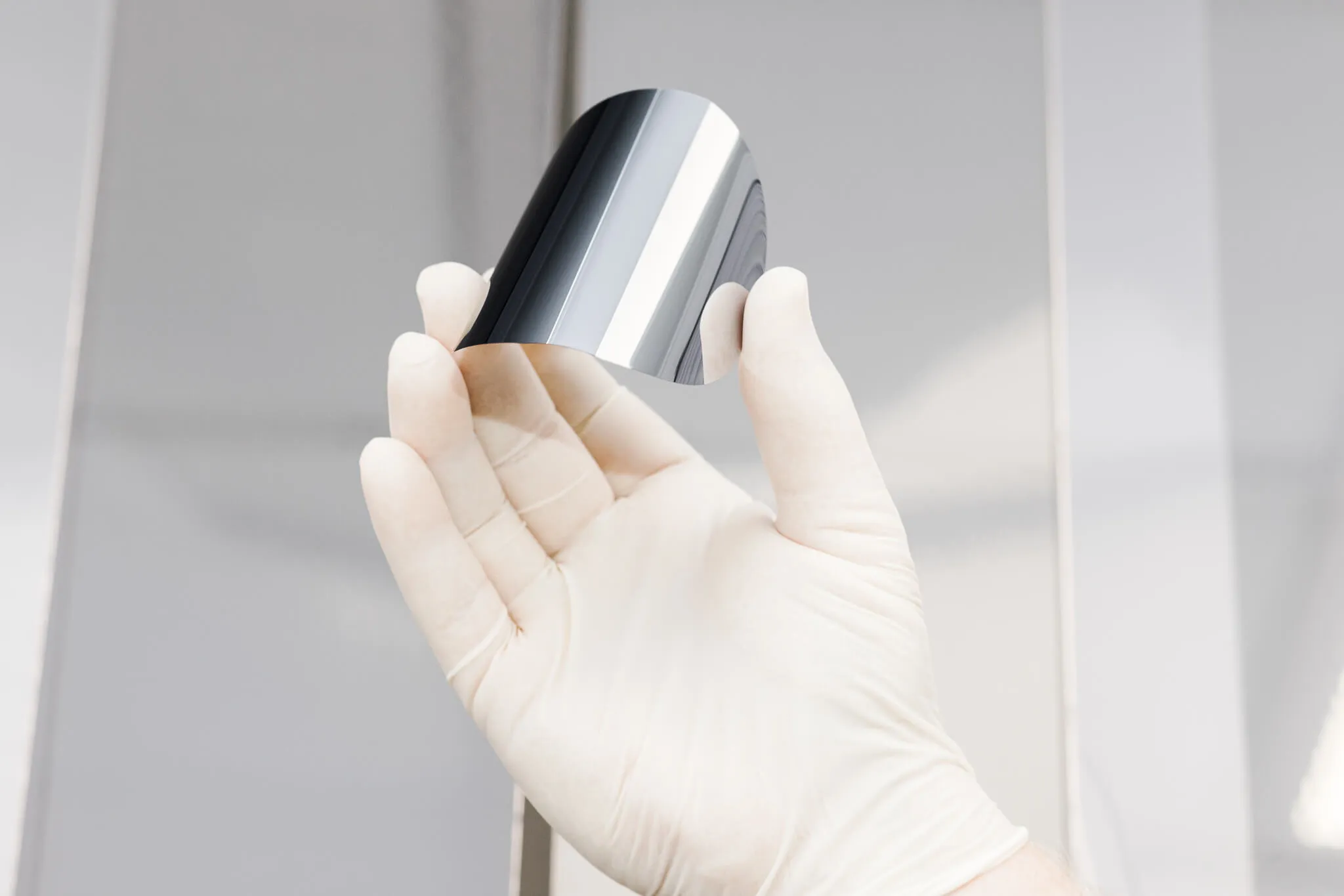
A semiconductor made of indium and phosphorus is called an indium phosphide wafer. Its crystal structure, face-centered cubic (also known as "zinc blende"), is the same as that of GaAs and the majority of III-V semiconductors.
White phosphorus and indium iodide can be combined directly at high temperatures and pressure to create indium phosphide. A trialkyl indium molecule and phosphide mixture can similarly be thermally decomposed to form indium phosphide. Because of its better electron velocity than the more popular semiconductors silicon and gallium arsenide, inP is utilized in high-power and high-frequency circuits.
Ultra-sensitive spectroscopic analyzers, polymer thickness measurements, and the detection of multilayer coatings in the automotive industry utilize optoelectronic terahertz technology.
High-speed microelectronics are also realized on indium phosphide wafers, and these semiconductor devices are now the fastest ones on the market. High Electron Mobility Transistors (HEMT) or heterostructure bipolar transistors are typically the foundation for microelectronics on InP.
InP substrates are used in photovoltaic cells with the highest efficiency, up to 46%, to create the best bandgap configuration and effectively convert solar light into electrical energy. Today, only InP substrates can produce the necessary low bandgap materials with high crystalline quality due to their high lattice constant.
Indium Phosphide (InP) is also utilized in photonic integrated circuits (PICs). Active laser generation, amplification, control, and detection features of InP photonic integrated circuits. They are the perfect part of communication and sensing applications because of this.
At Wafer World, our team can provide you with different high-quality semiconductors and other materials for your electronic needs. Contact us today to learn more about our products!


