August 26, 2025
Shop NowSeveral factors need to be considered when picking the right silicon wafer for your project. Crystal orientation plays a particularly crucial role. Silicon is a crystalline material whose atomic arrangement varies based on orientation. Different orientations have different electron and hole mobilities, resulting in different uses.
Anisotropic wafer etching behaves differently on different planes. For instance, (100) and (110) surfaces etch faster than (111), which acts as an etch stop. This is crucial for MEMS, trench isolation, and microfabrication steps where controlled etch profiles are needed.
The rate at which silicon dioxide (SiO₂) grows thermally depends on orientation. (100) silicon grows faster and more uniformly than (111). This impacts gate oxide thickness and dielectric properties in MOSFETs.
Dopant atoms (such as boron or phosphorus) diffuse along different crystallographic directions at different rates. Orientation affects junction depth and dopant profiles, impacting transistor performance.
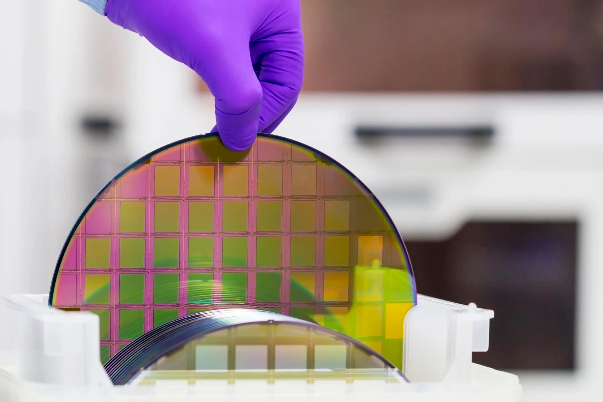
Crystal orientation in silicon wafers is critically important because it directly affects the wafer's electrical, mechanical, and chemical properties and, thus, the performance and yield of semiconductor devices built on them.
Whether you’re looking for substrates for CMOS technology or need to test some FinFET applications, different crystal orientations can offer different results. Do you still need help finding the right semiconductor for you? Contact Wafer World for some personalized tips!


