Epitaxial growth is a foundational step in modern wafer manufacturing, directly shaping device performance, yield, and long-term reliability. Whether you are producing logic devices, power electronics, optoelectronics, or compound semiconductors, the epitaxial method you choose determines not only material quality—but also throughput, cost structure, and scalability.
Three techniques dominate industrial and research environments today: LPCVD, MOCVD, and MBE. While they are often compared at a theoretical level, their real differences become clear only when viewed through the lens of manufacturing constraints and application requirements.
This guide breaks down how each method works, where it excels, and how to choose the right approach for your wafer manufacturing goals.
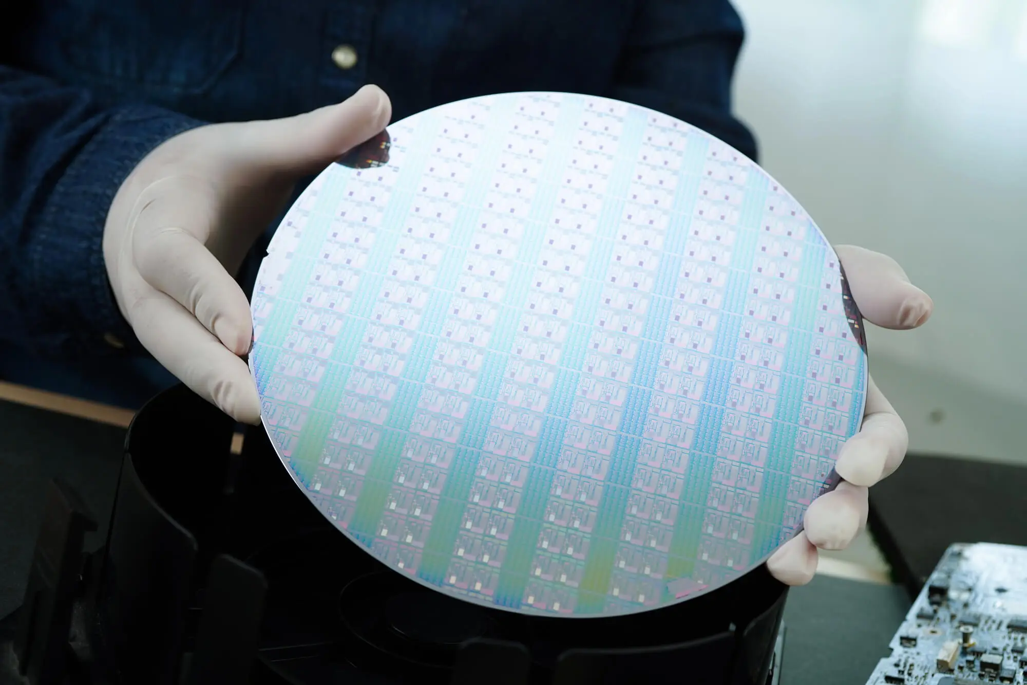
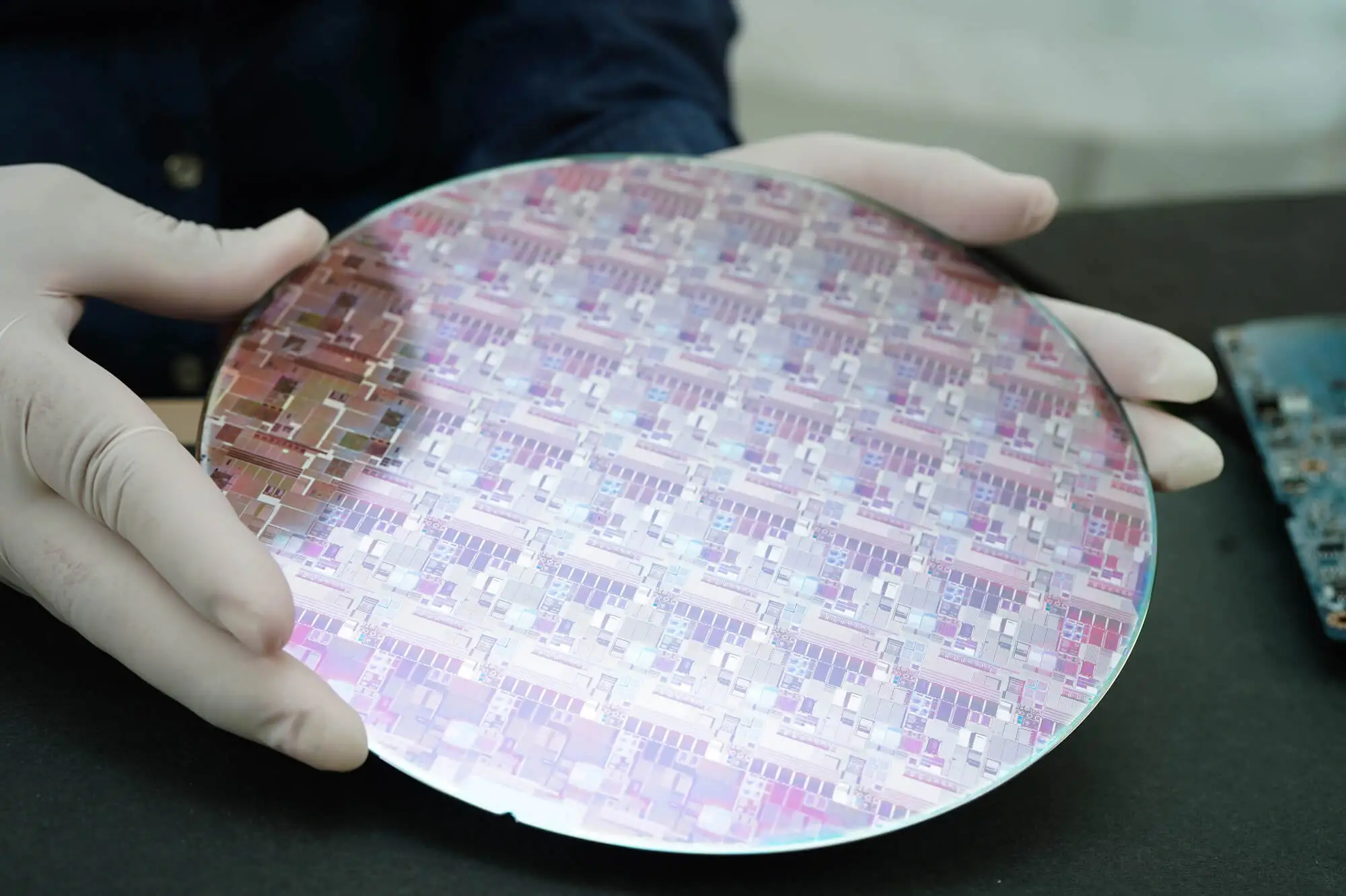
Epitaxy is the process of depositing a single-crystal layer on a crystalline substrate, such as silicon, SiC, GaAs, or sapphire, where the deposited layer maintains the crystal structure of the underlying wafer. This controlled crystal alignment is essential for achieving predictable electrical behavior and low defect densities.
Epitaxial growth is widely used to:
Different growth methods exist because no single technique optimizes precision, speed, cost, and material flexibility simultaneously.
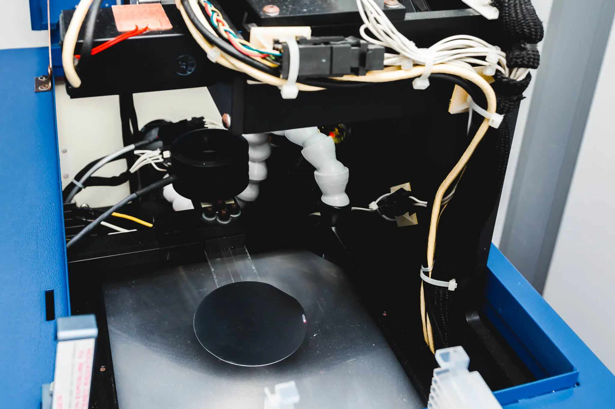
Low-Pressure Chemical Vapor Deposition (LPCVD) is commonly associated with silicon epitaxy in high-volume manufacturing environments.
In LPCVD, gaseous precursors react at elevated temperatures (typically 800–1,100 °C) under low pressure, forming a solid crystalline layer on the wafer surface. The low pressure improves film uniformity and reduces unwanted gas-phase reactions.
The strengths of LPCVD include:
On the other hand, some limitations of these processes include that they're primarily suited for silicon-based epitaxy and thus offer limited flexibility for complex compound semiconductors. Additionally, the high temperatures may not be compatible with all substrates.
LPCVD is ideal for logic, memory, and power silicon devices where cost efficiency and volume dominate decision-making. In wafer manufacturing lines focused on consistency and scale, LPCVD remains a workhorse technology.
Metal-Organic Chemical Vapor Deposition (MOCVD) is the most commonly used epitaxial method for III-V and wide-bandgap semiconductors, such as GaN, GaAs, and InP.
MOCVD employs metal-organic precursors and hydride gases that decompose on a heated substrate to form epitaxial layers with precise composition control. Growth occurs at moderate pressures and temperatures appropriate for the material system.
Some of the benefits of MOCVD are:
On the downside, it has higher operating costs due to the use of precursor materials and highly complex gas-handling and safety requirements. Additionally, it has a slightly lower atomic-level precision than MBE.
MOCVD dominates wafer manufacturing for LEDs, power electronics (GaN, SiC epitaxy), RF devices, and optoelectronics. It offers the best balance between precision and throughput for compound semiconductor production.
Molecular Beam Epitaxy (MBE) is known for unmatched precision and control, making it the gold standard for research and specialized device development.
In MBE, ultra-pure elemental sources are evaporated in an ultra-high vacuum chamber. Atomic or molecular beams travel directly to the wafer surface, allowing near-perfect control over layer thickness and composition.
The strengths of MBE are:
On the downside, this epitaxial growth method has very low growth rates alongside high capital and operating costs. This leads to limited throughput and scalability.
MBE excels in research labs, prototype development, quantum devices, and advanced III-V structures where precision outweighs cost and volume considerations.
The “best” epitaxial growth method is not universal—it depends on what you are manufacturing and why.
Epitaxial growth affects more than material quality—it influences lead times, equipment availability, and wafer sourcing strategies. Choosing a method aligned with your supply chain capabilities reduces bottlenecks and improves yield predictability.
This is why experienced wafer manufacturing partners don’t just supply substrates—they help align epitaxy, wafer specs, and downstream processing from the start.
Each epitaxial growth method serves distinct semiconductor applications, depending on the required precision, scalability, and material system.
Molecular Beam Epitaxy (MBE) is primarily used in research, prototyping, and advanced electronic structures where atomic-level control is essential. It is widely applied in the fabrication of quantum wells, superlattices, tunnel junctions, and low-dimensional structures for optoelectronics, spintronics, and quantum computing.
Because of its ultra-high vacuum environment and slow growth rates, MBE is ideal for III-V compound semiconductors such as GaAs and InP in laboratory and niche production settings.
Metal-Organic Chemical Vapor Deposition (MOCVD) dominates high-volume manufacturing of compound semiconductor devices. It is the preferred method for producing GaN and SiC epitaxial layers used in LEDs, laser diodes, RF components, and power electronics.
MOCVD enables excellent thickness uniformity, high throughput, and scalability, making it the industry standard for commercial wafer production.
Low-Pressure Chemical Vapor Deposition (LPCVD) is commonly used in silicon-based manufacturing where uniformity and process stability are critical. It supports the growth of silicon epitaxial layers, polysilicon films, and dielectric coatings used in CMOS devices, MEMS sensors, and integrated circuits, particularly in large-scale semiconductor fabrication.
LPCVD, MOCVD, and MBE all play important roles in modern wafer manufacturing. Understanding their tradeoffs enables engineers and decision-makers to optimize not only individual devices, but entire production ecosystems.
When epitaxial growth is chosen strategically, it becomes a competitive advantage rather than a limitation. Do you need help procuring high-quality wafers before epitaxial growth? Contact Wafer World for support and innovative semiconductor products!


