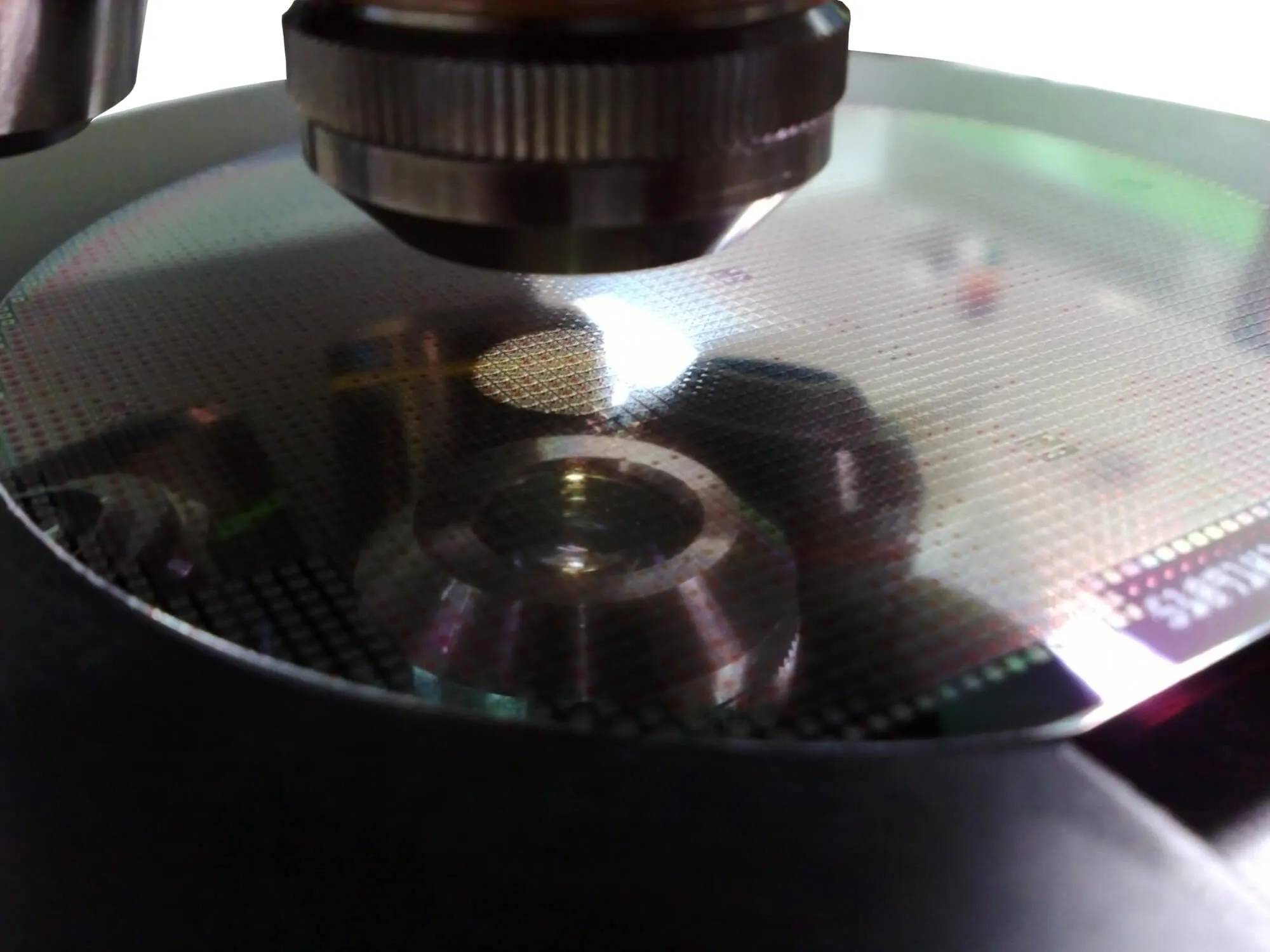
While silicon wafers are the most commonly used semiconductor, partly thanks to the massive amounts of silicon in the world, some other types provide their own unique advantages. One of these is a GaAs wafer, which stands for “gallium arsenide.” At Wafer World, no matter which type of wafer you’re interested in, we always strive for a high-quality product. Our wafers always undergo intense testing, so you are left with wafers you are satisfied with. There’s a lot to know about gallium arsenide wafers, so if you’re interested in how these thin semiconductors are a huge part of today’s technology, let’s take a closer look into what they are and how they’re used.

A compound of the elements gallium and arsenic creates gallium arsenide, or GaAs. Just like silicon, gallium arsenide is a semiconductor that is used to create wafers. GaAs crystals can be created through three different methods. One of the more common methods is the vertical gradient freeze process, which involves growing crystals and slicing them, followed by edge rounding and polishing them into wafers. Another method is the Bridgman-Stockbarger technique. For this process, polycrystalline material is heated to its melting point and cooled. While the technique is a consistent way to produce crystal ingots, its drawback is the lack of reliability. The properties of the crystal are not guaranteed to be uniform. Finally, there’s the Czochralski method, which is also commonly used with silicon and germanium. To begin the process, a crystal is dipped into molten GaAs with a rod, then the rod is pulled and rotated.
In 1250 AD, alchemist Albertus Magnus, who was also known as Saint Albert the Great, discovered arsenic. Hundreds of years later, in 1875, a French chemist named Paul-Emile Lecoq de Boisbaudran discovered the chemical element gallium while studying Zinc. He originally named it “gallia” after his home country. France was first called Gaul, which translates to “Gallia” in Latin. Using Dmitri Mendeleev’s periodic trends as a guide, Lecoq de Boisbaudran figured that there must be an element right next to zinc. He thoroughly examined zinc ore and made the discovery. With the two of these discoveries combined, gallium arsenide was created. While gallium arsenide was discovered much earlier, the first GaAs microprocessors were not used until the early 1980s. They were created by the RCA corporation and were close to being used in the Star Wars program. The Star Wars program was a nickname for the Strategic Defense Initiative, which was a missile defense system proposed by the U.S. Department of Defense in 1984.
A lot of people know about silicon wafers since they’re so commonly used, but sometimes the alternative can be the better option. With a variety of wafers such as germanium and GaAs, it’s best to look at the pros and cons to discover how they can best be utilized.
Since silicon is a very abundant resource, silicon wafers are going to be a more inexpensive option, however, GaAs wafers have plenty of benefits that make them a very capable choice – sometimes an even better one depending on what you’ll be using them for.
GaAs has a direct band gap, which contrasts from silicon having an indirect bandgap. This means that silicon does not handle light emission well, while GaAs is really good at both emitting and absorbing light. This characteristic makes GaAs wafers the perfect substrate for space exploration.
A perk that comes alongside the bandgap is that GaAs wafers are more resistive than silicon wafers. Combining GaAs with a high relative permittivity or dielectric constant will create the opportunity for a great substrate with natural isolation between the circuits and devices.
Gallium arsenide has many other advantages over silicon that you might not have known about. Some of these include:
As you can see, while silicon wafers may be a more inexpensive option, sometimes you may need to factor a better functionality into your situation. With GaAs wafers, you’ll be getting many benefits that you simply won’t receive from silicon.

GaAs wafers may be a great choice for some applications, but sometimes silicon is still going to be your best go-to option. Here are some advantages that silicon has over GaAs.
As we’ve already established, silicon is much more inexpensive. This is partly due to its abundance and partly due to how cheap it is to process.
An electron-hole is a term used to describe a missing electron at a location where it could theoretically exist inside an atom. It is able to create an electric current within a semiconductor. Compared to GaAs, silicon has a significantly higher electron-hole mobility. This is essential for complementary metal-oxide-semiconductor logic, allowing for the fabrication of P-channel field-effect transistors, which are of a much higher speed. In contrast, circuits that utilize GaAs wafers use much more power.
Unlike GaAs, silicon can use silicon dioxide as an insulator, which can be easily placed on circuits. This native oxide allows for much more stable support of an insulating layer.
GaAs wafers have many opportunities to be used for a wide variety of electronic, solar, and light-emission applications. Some of these applications include but are not limited to:

When you need wafers, it’s always best to be properly informed of which one is right for you. Even if silicon and GaAs will both be a usable option for the desired application, the experts at Wafer World have an immense amount of inside knowledge. We’ll be able to point you in the right direction. If you are ready to take advantage of what GaAs wafers have to offer, Wafer World has you covered. With our high-quality care and precision, our wafers meet the standards you expect. If you’re interested in making a purchase, contact us today to learn more.


