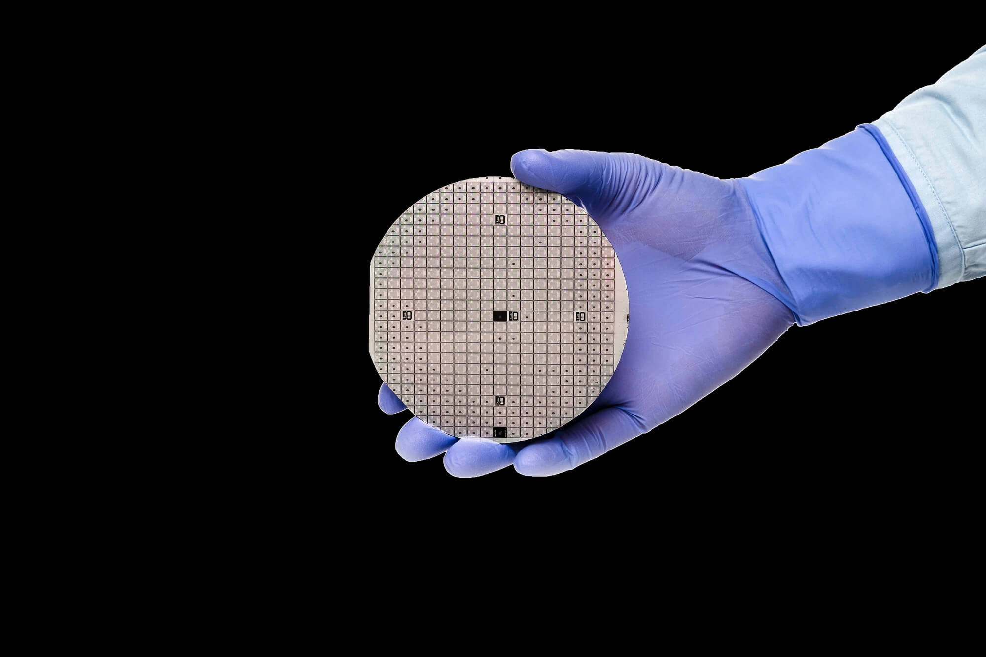
InP reclaim wafers are essential for high-speed photonics, optoelectronics, and 5G applications. But integrating InP with silicon or other substrates can be quite a challenge, requiring a precise bonding process that both preserves material integrity and maintains electrical and optical performance.
Understanding how InP wafer bonding works—and how to optimize it—can make the difference between yield loss and scalable, production-ready results.
In order to join two ultra-flat surfaces—typically InP-to-InP, InP-to-Si, or InP-to-glass—without sacrificing device performance, InP wafers must be bonded. Usually, the procedure consists of three crucial steps:
Successful InP wafer bonding expands design possibilities for lasers, detectors, and transceivers. By integrating InP with silicon photonics, manufacturers can combine the optical efficiency of InP with the scalability of Si-based processing—driving faster, smaller, and more energy-efficient devices.
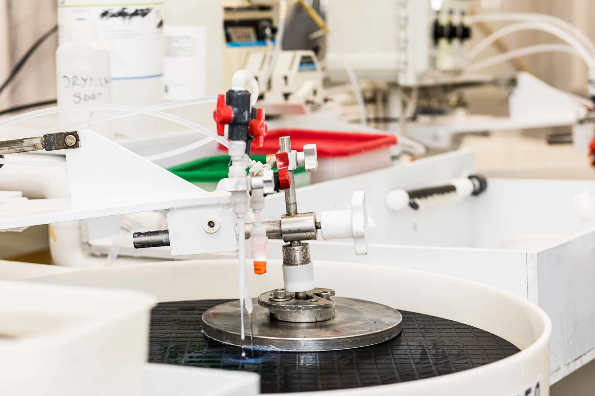
Achieving consistent InP wafer bonds demands more than equipment—it requires process expertise, cleanroom discipline, and materials science insight.
At Wafer World, we provide tailored InP bonding solutions backed by real-time process data, validated recipes, and proven yield results. If you’d like to learn more about our products, contact us today and let’s discuss your bonding challenge!


