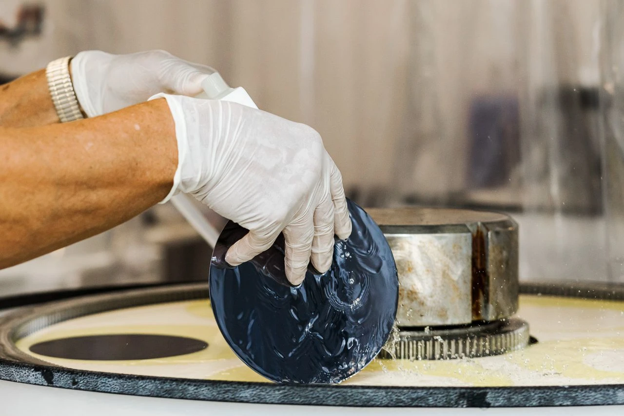
Modern technology depends heavily on semiconductor materials that support reliable electrical performance and precise device functionality. Smartphones, medical equipment, industrial automation systems, and communication devices all rely on carefully engineered semiconductor components to operate efficiently. One of the most important materials behind these technologies is the Si wafer, which serves as the foundational substrate for countless electronic and microelectronic applications.
Silicon wafers are valued for their electrical stability, thermal resistance, and compatibility with advanced fabrication processes. These properties enable manufacturers to fabricate integrated circuits, sensors, transistors, and power devices with high precision. As electronics continue to shrink and become more powerful, wafers remain central to innovation across many industries.
Understanding how silicon wafers are used can help manufacturers, engineers, researchers, and procurement teams evaluate material requirements more effectively. Each application places different demands on wafer quality, crystal orientation, surface finish, and conductivity.
Silicon wafers act as the base material for integrated circuits and semiconductor devices. During fabrication, multiple electronic components are built layer by layer onto the wafer surface using advanced lithography, etching, and deposition techniques.
The electrical behavior of silicon makes it highly suitable for semiconductor applications. Manufacturers can carefully modify conductivity through doping processes that introduce controlled impurities into the material. This flexibility enables wafers to support transistors, diodes, and complex circuitry.
Consumer electronics rely heavily on these semiconductor components. Smartphones, laptops, tablets, gaming systems, and wearable devices all contain integrated circuits fabricated on silicon substrates. Without wafers, the compact electronic systems used daily would not be possible.
Integrated circuits combine millions or even billions of transistors onto a single chip. Silicon wafers provide the stable foundation necessary for building these miniature structures with precision.
The manufacturing process requires extremely smooth and defect-free surfaces. Even microscopic imperfections may affect device reliability or reduce production yields. For this reason, wafer flatness, purity, and surface quality are carefully monitored throughout fabrication.
Different crystal orientations also influence processing performance. Common orientations such as <100> and <111> support specific etching behaviors and electrical characteristics used in circuit manufacturing.
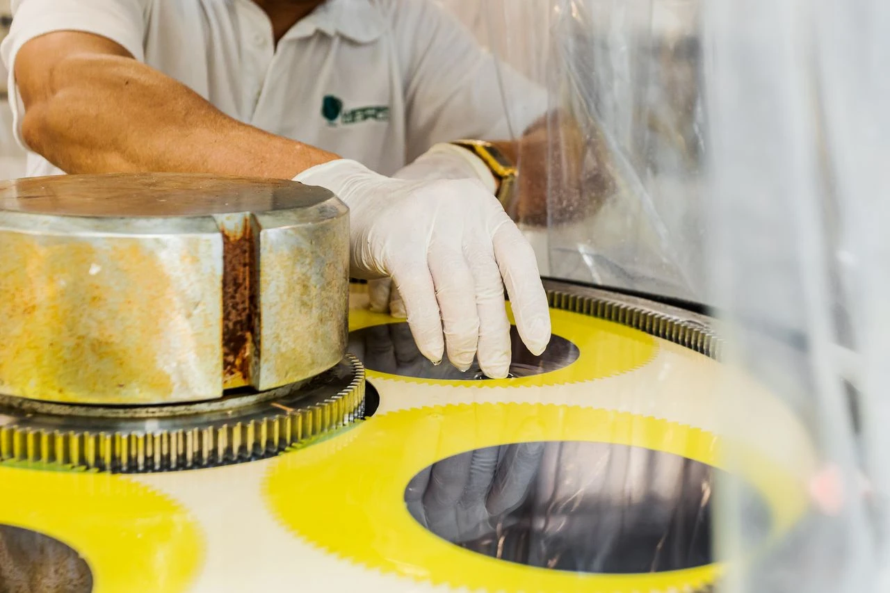
Silicon wafers are widely used in sensor production because they can respond to electrical, thermal, optical, and mechanical changes. Sensors fabricated on silicon substrates help electronic systems collect and process real-world data.
Pressure sensors, temperature sensors, accelerometers, and motion detectors all rely on semiconductor structures formed on wafers. These components are commonly found in vehicles, industrial systems, healthcare equipment, and consumer electronics.
Medical devices frequently use sensor technology to monitor patient conditions, measure biological signals, and support diagnostic procedures. Industrial automation systems also rely on sensors to monitor equipment performance and maintain production efficiency.
Microelectromechanical systems (MEMS) combine mechanical structures with electronic circuitry on silicon substrates. These tiny devices can detect movement, pressure, vibration, or environmental changes.
MEMS technology is commonly used in smartphones, automotive safety systems, drones, and navigation equipment. Accelerometers and gyroscopes in mobile devices are examples of MEMS components fabricated from silicon wafers.
The precision of wafer processing allows manufacturers to create highly compact devices while maintaining stable performance. This miniaturization continues driving advancements in portable electronics and smart technologies.
Microchips are produced through highly controlled fabrication procedures involving multiple processing stages. Silicon wafers move through cleaning, oxidation, photolithography, ion implantation, deposition, and etching steps before becoming finished semiconductor devices.
Photolithography transfers intricate circuit patterns onto the wafer surface using light-sensitive materials and precision imaging systems. These patterns define the electrical pathways and transistor structures within the chip.
Etching removes selected regions of material to create desired circuit geometries, while deposition adds thin layers for conductivity and insulation. Each process must remain carefully controlled to achieve accurate device performance.
Semiconductor fabrication environments require exceptionally pure materials. Contaminants or particles can interfere with electrical behavior and damage circuit structures.
Manufacturers inspect wafers for scratches, particles, pits, and surface irregularities before processing begins. Advanced inspection systems help identify defects that may reduce production efficiency.
Flatness is also critical because uneven surfaces can create alignment issues during photolithography. Tight thickness tolerances and low warp measurements help maintain stable processing conditions throughout fabrication.
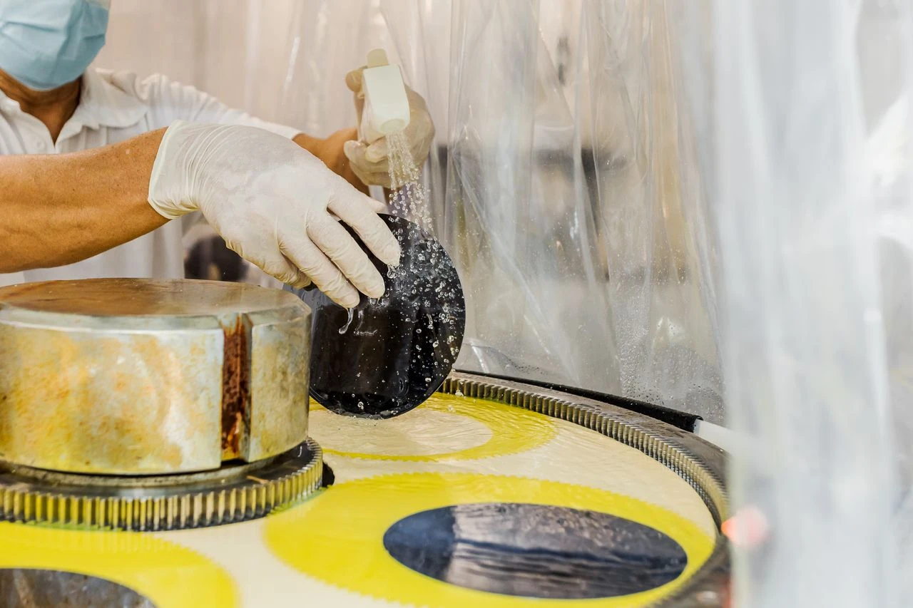
Automotive technologies increasingly rely on semiconductor components fabricated on silicon substrates. Modern vehicles contain electronic control units, driver assistance systems, safety sensors, and communication modules that depend on reliable semiconductor performance.
Electric vehicles also require advanced power electronics capable of managing battery systems, charging operations, and energy conversion processes. Silicon-based semiconductor devices support these demanding electrical environments.
Industrial automation systems use wafers in programmable controllers, robotic equipment, machine monitoring systems, and industrial sensors. These applications require components that can operate reliably over the long term in production conditions.
Communication infrastructure depends heavily on semiconductor technologies. Data centers, wireless networks, satellite systems, and internet hardware all use microchips fabricated on silicon substrates.
Processors, memory devices, and networking components enable modern communication systems to handle large amounts of digital information efficiently. As data demands continue to increase, semiconductor manufacturing remains essential to maintaining technological growth.
Research institutions also use silicon wafers in experimental electronics, photonics, and advanced materials development. These projects help support future innovations in computing, energy systems, and sensing technologies.
Different applications require specific wafer characteristics depending on electrical performance, processing methods, and environmental conditions. Factors such as resistivity, crystal orientation, diameter, and surface finish all influence material suitability.
Prime-grade wafers are commonly used for advanced semiconductor production because they meet strict quality standards. Test grade and reclaim wafers may support equipment calibration, process monitoring, or research environments.
Proper material selection helps reduce production risks and improve fabrication consistency. Carefully reviewing wafer specifications can improve compatibility with manufacturing equipment and device requirements.
Organizations working with semiconductor materials often prioritize long-term supply consistency and traceability. Stable wafer specifications across production cycles help maintain reliable process control and predictable manufacturing outcomes.
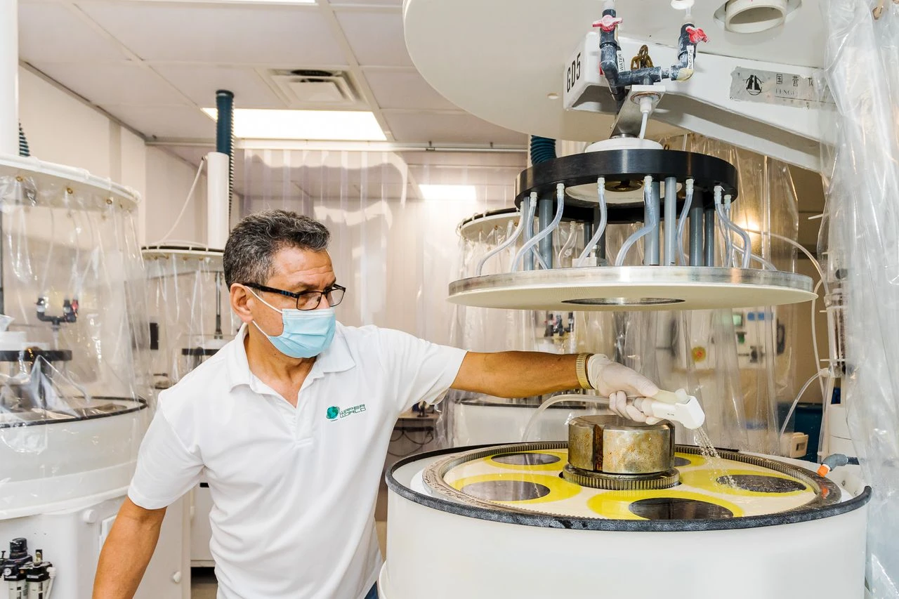
Silicon wafers continue to support the technologies that power communication systems, industrial automation, medical devices, sensors, and microchips worldwide. Whether the focus is semiconductor fabrication, MEMS production, or advanced electronics development, understanding wafer applications can help organizations make more informed material decisions.
If your team is evaluating materials for Si wafer applications, reviewing technical specifications and production requirements can help ensure more reliable long-term results. Wafer World provides silicon wafer solutions for semiconductor, research, and industrial applications. Contact us today to discuss your project needs or connect with our team for additional information.




