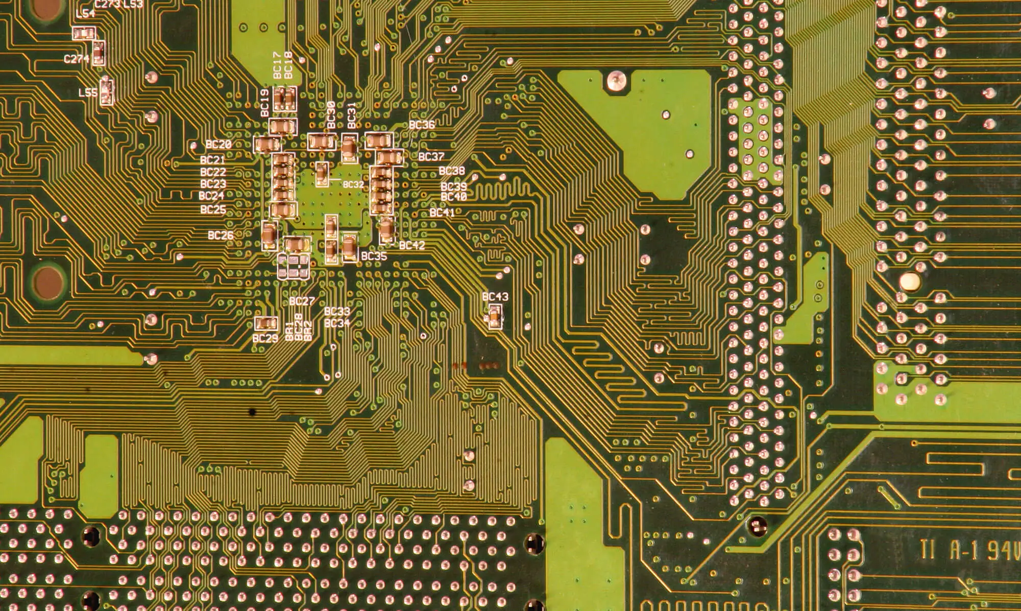
Today's smart technologies rely on Micro-Electro-Mechanical Systems (MEMS), which range from pressure sensors in automotive systems to motion detectors in smartphones. This innovation is built around one critical component: thin silicon wafers.
These ultra-flat, ultra-pure substrates enable the creation of precise, miniaturized devices with excellent mechanical and electrical performance.
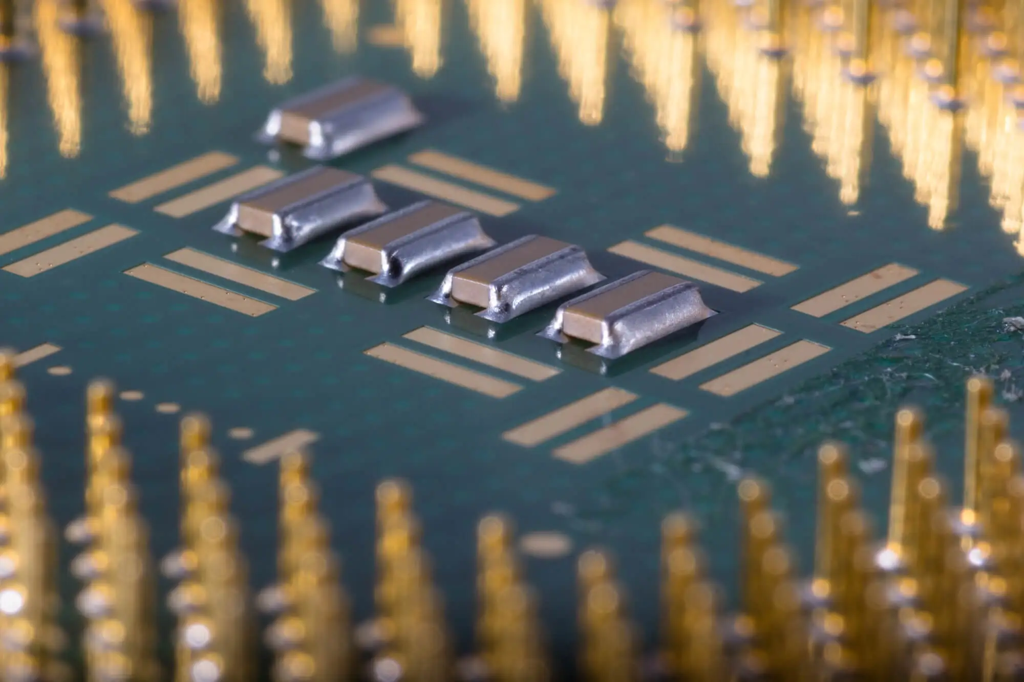
MEMS devices are composed of mechanical elements, sensors, and electronics on a single silicon substrate. To achieve this level of integration and miniaturization, wafer thickness is critical.
Thin silicon wafers (typically between 100 µm and 300 µm) offer several fabrication advantages:
In short, thin wafers are more than just a mechanical requirement; they also improve performance.
Thin silicon wafers enable a variety of MEMS technologies across industries:

As demand for miniaturization and functionality continues to grow, thin silicon wafers will remain the foundation of MEMS innovation. From autonomous vehicles to wearable medical devices, every breakthrough begins with a thin substrate designed for excellence.
To give your products a competitive edge in this rapidly evolving market, partnering with a wafer supplier that understands the intersection of materials science and microfabrication is crucial. At Wafer World, we aim to support technological companies in the Palm Beach area—and country-wide.
Would you like to learn more about our product’s specs? Contact us today for a personalized quote!


