Thin silicon wafers play a vital role in the development of MEMS (Microelectromechanical Systems) and sensor technologies, which are integral to modern electronics. These ultra-thin silicon slices are not only crucial for achieving miniaturization but also for enhancing the precision and performance of electronic devices.
As the tech industry moves toward smaller, faster, and more efficient systems, the importance of thin silicon wafers cannot be overstated.
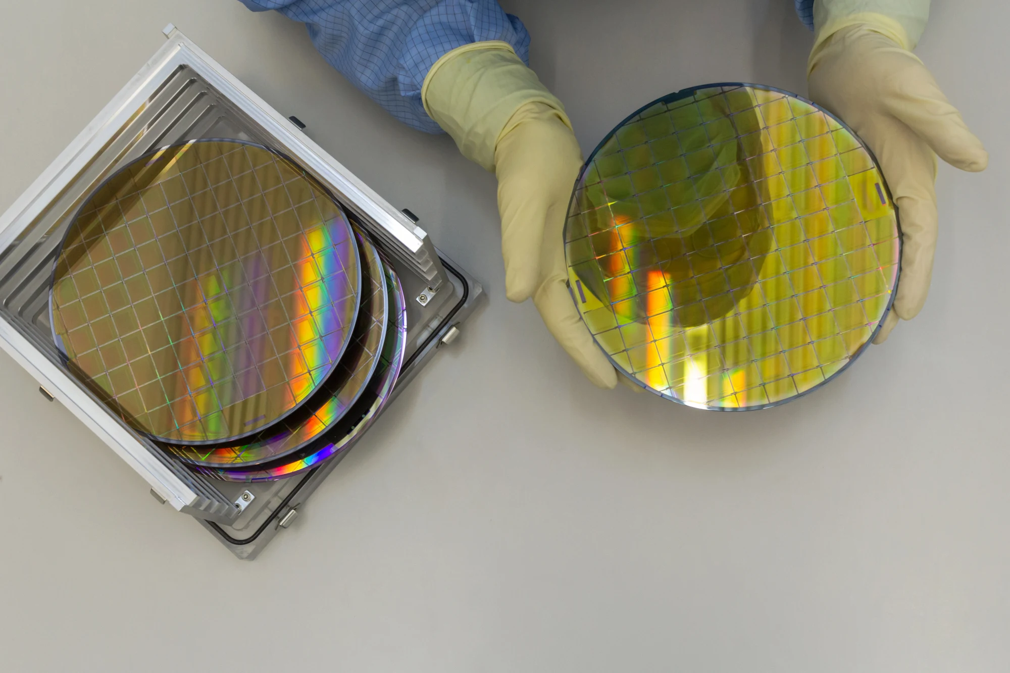
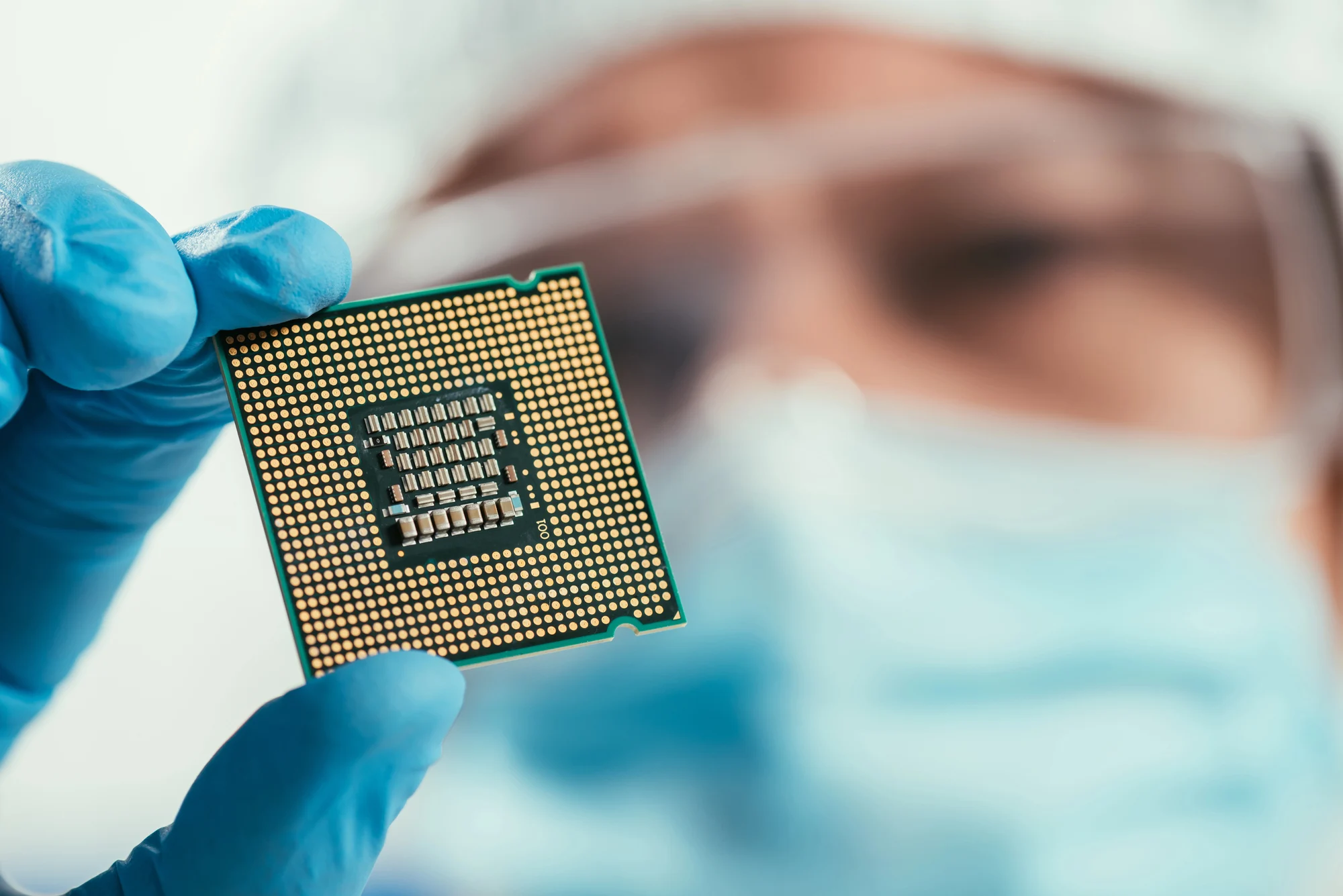
Thin silicon wafers are slices of silicon material that are manufactured with a reduced thickness compared to traditional wafers. These wafers serve as the substrate for various semiconductor devices, including MEMS and sensors.
By reducing the wafer’s thickness, manufacturers can achieve higher performance, better heat dissipation, and greater precision, all of which are essential for advanced technological applications.
The thin nature of these wafers enables their integration into miniature devices, making them ideal for applications where size, weight, and power efficiency are crucial.
The process of manufacturing thin silicon wafers begins with standard silicon wafers, which are thinned using advanced techniques. These processes involve mechanical grinding, polishing, and etching, all of which remove material from the wafer’s surface to achieve the desired thickness.
Once the wafer reaches the required thinness, it undergoes rigorous quality control checks to ensure uniformity and performance. This precision ensures that the wafers are suitable for applications such as MEMS, where even slight variations can affect device functionality.
MEMS are miniature devices that combine mechanical components with electrical elements, enabling them to perform specific tasks like sensing, actuation, and communication. These devices are widely used in industries such as automotive, healthcare, telecommunications, and consumer electronics.
Thin silicon wafers are ideal for MEMS applications because they allow for the integration of numerous micro components within a small footprint. MEMS accelerometers, for example, are used in smartphones for motion sensing and in automotive systems for airbag deployment and stability control.
Additionally, MEMS pressure sensors in the automotive industry rely on thin silicon wafers to accurately measure air pressure in tires, while MEMS microphones in consumer electronics benefit from the precise sensitivity of these wafers, delivering high-quality audio.
Sensors are the backbone of many modern devices, detecting everything from temperature and motion to pressure and even chemical composition. Thin silicon wafers are commonly used in the manufacture of various types of sensors due to their excellent electrical and mechanical properties.
For example, in the medical field, thin silicon wafers are used to produce biosensors that detect glucose levels in diabetic patients or monitor other health parameters.
In consumer electronics, thin silicon wafers enable sensors in wearables, like fitness trackers, that measure heart rate, steps, and calories burned. The thinness of these wafers enables the creation of small, lightweight sensors that are both energy-efficient and high-performing.
Thin silicon wafers offer distinct advantages for enhancing the performance of MEMS (Microelectromechanical Systems) devices. Due to their reduced thickness, they enable more precise control over mechanical and electrical properties, which is critical for MEMS applications that require high sensitivity and accuracy.
Thin silicon wafers also improve the overall functionality and durability of MEMS devices, especially in harsh environments such as automotive or industrial systems.
For example, in pressure sensors used in automotive safety systems, the reduced thickness of the silicon wafer helps ensure faster response times and increased reliability under fluctuating conditions.
The wafers also enhance the precision of MEMS accelerometers, which are critical in devices such as smartphones, wearables, and medical instruments. Their ability to withstand extreme temperatures and vibrations ensures that MEMS devices continue to operate with the utmost efficiency, delivering better user experiences and higher-quality results in complex systems.
One of the key benefits of thin silicon wafers is their role in sensor miniaturization. As devices become increasingly smaller, thin silicon wafers allow manufacturers to create high-performance sensors that are compact yet capable of delivering precise results.
This miniaturization is essential in industries like consumer electronics, healthcare, and environmental monitoring, where small, efficient devices are in high demand.
In the healthcare industry, for instance, thin silicon wafers are used to produce wearable health monitors that track vital signs in real-time. These devices need to be small enough for continuous use but still offer the sensitivity and reliability required for accurate data collection.
Similarly, in the environmental sector, thin silicon wafers enable the creation of sensors that monitor air quality or detect pollutants, making them essential for smart city infrastructure.
The ability to integrate sensors into small form factors while maintaining performance is a direct result of using thin silicon wafers.
Thin silicon wafers offer several key benefits that make them indispensable in MEMS and sensor technologies:
As electronics continue to evolve, the demand for smaller, more powerful devices increases. Thin silicon wafers are at the forefront of this revolution, enabling the development of smaller, faster, and more energy-efficient devices.
Whether it’s in smartphones, medical devices, or automotive systems, thin silicon wafers are paving the way for next-generation technologies.
Their unique properties, including superior conductivity, mechanical strength, and ease of integration, make them indispensable for engineers designing cutting-edge MEMS and sensors.

At Wafer World, we specialize in high-quality thin silicon wafers ideal for MEMS and sensor applications. Our wafers are designed to meet the precise needs of engineers and manufacturers, ensuring optimal performance and reliability in every project.
With our advanced manufacturing processes, we provide the ideal materials that enable the creation of cutting-edge technology.
Contact us today to discuss your specific needs and learn how our advanced wafers can help you stay ahead of the competition.


