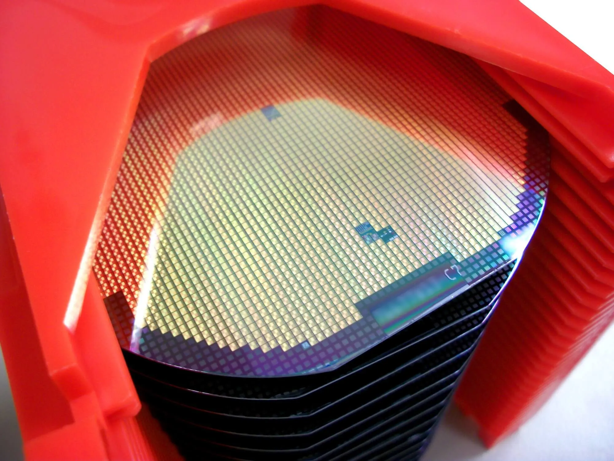
Laser marking on wafers is an essential practice within the semiconductor industry, offering a precise and efficient method for marking various materials used in electronic devices. Essentially, laser marking involves using highly focused laser beams to create marks, patterns, or identifiers on the surface of semiconductor wafers. This process is crucial for identification, traceability, and quality control throughout the production chain.
Laser marking provides unparalleled precision, enabling manufacturers to create intricate patterns or markings on wafers with micron-level accuracy. This precision is vital for guaranteeing the functionality and reliability of semiconductor devices.
Laser marking is a non-contact process, unlike traditional marking methods such as etching or mechanical engraving. This eliminates the risk of physical damage to delicate wafers and ensures consistent quality across production batches.
Laser marking systems operate at high speeds, allowing manufacturers to mark wafers rapidly without compromising accuracy. This efficiency is essential for meeting the demands of high-volume production environments.
Laser marking is commonly used to imprint unique identifiers such as serial numbers, barcodes, or DataMatrix codes directly onto semiconductor wafers. These identifiers enable precise tracking and traceability throughout the manufacturing process and supply chain.
Manufacturers often use laser marking to add branding elements, logos, or product information onto wafers. These markings serve as a means of branding and differentiation in the competitive electronics market.
Laser marking creates alignment marks or patterns on wafers, facilitating precise alignment during subsequent manufacturing processes such as lithography or wafer bonding.
Laser marking can be utilized to mark wafers with quality control indicators such as pass/fail labels or inspection codes. These markings aid in identifying defective or out-of-specification wafers.
Laser marking on wafers is pivotal in semiconductor manufacturing because it provides precise, efficient, and versatile marking solutions. Its importance spans various applications, including identification, branding, alignment, and quality control, contributing to producing reliable and high-performance electronic devices.
With Wafer World, you are sure to get top-quality laser-marked products! Call us to order!


