
Semiconductor manufacturing is a highly precise and resource-intensive industry. The production of semiconductor wafers, such as Indium Phosphide (InP) wafers, involves cutting-edge technology and demands high-quality materials. However, it also generates a significant amount of waste. In recent years, innovations in wafer reclamation, especially in the context of InP reclaim wafers, have been driven by nanotechnology and beyond. These innovations hold promise not only for cost reduction but also for the sustainability of the semiconductor industry.
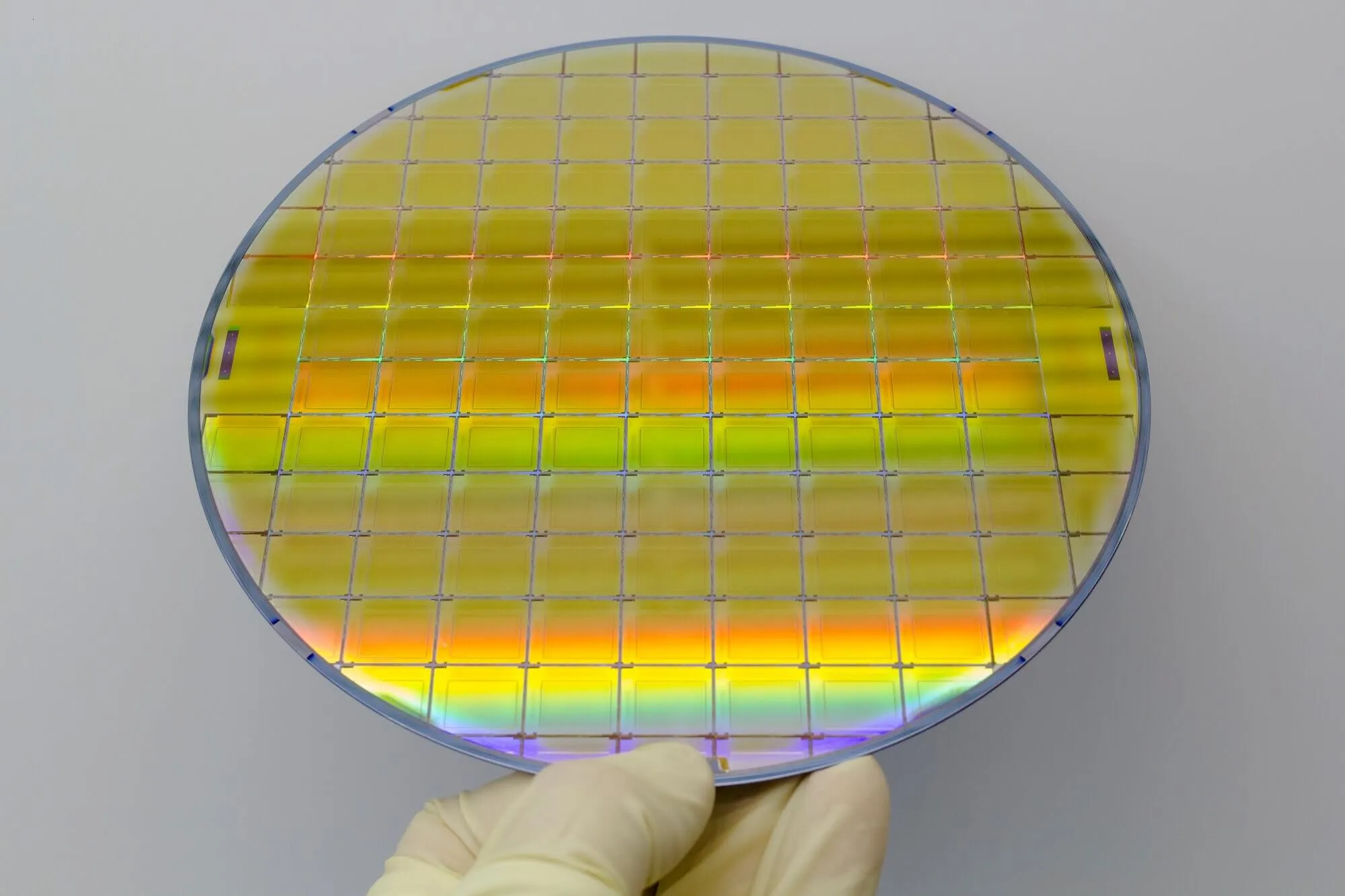
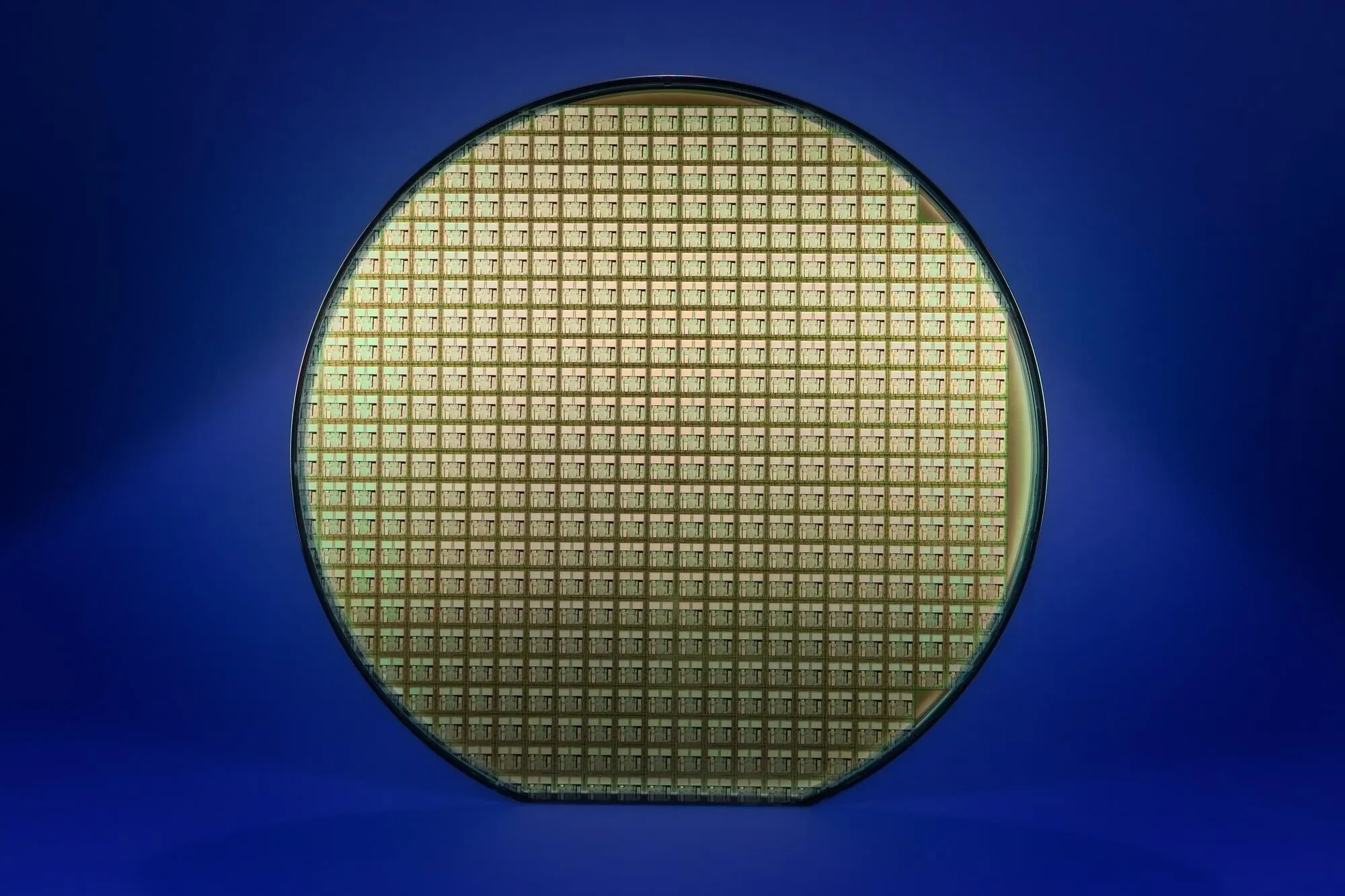
InP wafers are highly prized in the semiconductor industry for their excellent electronic and optoelectronic properties, making them ideal for applications like high-frequency transistors, lasers, and photodetectors. However, the manufacturing process generates a considerable amount of waste InP material in the form of defective or obsolete wafers. Traditionally, these wafers were discarded, contributing to the environmental burden and increasing production costs.
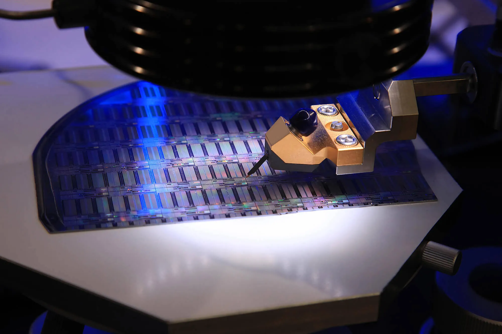
Nanotechnology, with its ability to manipulate materials at the nanoscale, has opened up new possibilities for InP wafer reclamation. Here's how it's making a difference:
Nanotechnology enables precise etching and cleaning of InP wafers, removing defects and contaminants at the nanoscale. This level of precision allows manufacturers to salvage wafers that would have been discarded in the past.
Nanoparticles and nanomaterials can be used to repair defects on InP wafers. This innovative approach involves depositing nanoscale materials onto the damaged areas, effectively "healing" the wafer and restoring its functionality.
Nanotechnology-driven thinning techniques have been developed to reduce the thickness of InP wafers without compromising their structural integrity. This not only reclaims wafers but also makes them suitable for new, advanced applications.
Nanotechnology has improved the testing and quality control processes for reclaimed InP wafers. Advanced nanoscale sensors and inspection methods ensure that only high-quality wafers are reintegrated into the production process.
While nanotechnology has already brought significant improvements to InP wafer reclamation, the journey is far from over. Beyond nanotechnology, other innovations are on the horizon.
AI-powered systems can analyze vast amounts of data generated during the reclamation process, helping to optimize every step. Machine learning algorithms can predict defects, guide repair processes, and enhance the overall efficiency of wafer reclamation.
Quantum dots and other advanced materials are being explored for their potential in reclamation and enhancing the performance of InP wafers. These materials may lead to new applications and improved wafer properties.
InP wafers are key components in solar cells and other green energy technologies. Innovations in reclamation will play a crucial role in making renewable energy more sustainable by reducing waste and production costs.
There are many innovative applications for InP Wafer Reclamation. Below are some notable ones.
InP wafers are at the forefront of next-generation electronics, including high-speed communication devices and advanced microprocessors. The innovations in InP wafer reclamation extend the lifespan of these wafers, ensuring a steady supply of high-quality materials for the production of cutting-edge electronics.
InP wafers are prized for their use in photonic and optoelectronic devices, such as lasers, optical amplifiers, and photodetectors. By leveraging nanotechnology and other innovations in reclamation, manufacturers can access cost-effective, reclaimed InP wafers that maintain the precision required for these applications.
As quantum computing research advances, InP wafers are being explored for their potential in quantum dot qubits. Innovations in wafer reclamation ensure a sustainable supply of InP material for the development of quantum processors, which could revolutionize computing as we know it.
InP wafers are crucial components in high-efficiency solar cells. Innovations in reclamation not only reduce the environmental impact of solar cell production but also contribute to lowering the cost of solar energy, making it a more accessible and sustainable energy source.
InP wafers find applications in medical devices such as sensors and imaging equipment. Innovations in reclamation make it possible to produce cost-effective medical devices without compromising on quality, potentially advancing healthcare technology.
Inp Wafer Reclamation has various environmental and economic benefits to ensure that you are helping Mother Earth.
One of the most significant advantages of InP wafer reclamation is the reduction in electronic waste. By salvaging and reusing wafers that would otherwise be discarded, the semiconductor industry contributes to a more sustainable and environmentally friendly approach to manufacturing.
InP wafers are expensive to produce, and reclaiming them presents a cost-effective alternative. Manufacturers can significantly reduce their production costs by incorporating reclaimed wafers into their processes, thus improving their overall profitability.
Innovations in reclamation align with the principles of a circular economy. They reduce the need for new InP material extraction and processing, conserving valuable resources and energy throughout the semiconductor manufacturing supply chain.
Semiconductor manufacturers who adopt advanced reclamation technologies can enhance their competitiveness on a global scale. By reducing costs and promoting sustainability, they can maintain a strong market presence and stay ahead in a rapidly evolving industry.
InP wafer reclamation contributes to energy efficiency in semiconductor manufacturing. The production of new wafers requires a substantial amount of energy, including the growth of crystalline structures and the various processing steps involved. Reclaiming wafers reduces the need for energy-intensive manufacturing, lowering the overall carbon footprint of the semiconductor industry.
Beyond the direct benefits to InP wafers, innovations in reclamation set a precedent for resource conservation in the broader electronics industry. As semiconductor manufacturers adopt more sustainable practices, they promote responsible resource management and encourage other industries to follow suit.
Innovations in InP wafer reclamation, driven by nanotechnology and other cutting-edge technologies, are revolutionizing the Wafer World. These advancements not only reduce costs but also contribute to a more sustainable and environmentally friendly manufacturing process. As technology continues to evolve, we can expect even more exciting developments in the field of wafer reclamation, further enhancing the efficiency and sustainability of semiconductor production. InP wafers, once seen as waste, are now becoming a valuable resource for the industry's future growth and innovation. Contact us to order!


