During the silicon wafer manufacturing process, laser marking has a crucial role. A beam of concentrated light is used through a laser machine to create a permanent mark on semiconductor packages.“Laser” isn’t just a normal word, but an acronym that stands for “Light Amplification by the Stimulated Emission of Radiation.” An atom is stimulated to produce light particles that are concentrated and directed. This is completed through the laser marking machine, and it can be programmed to exact specifications.Wafers are laser marked in order to trace them through the manufacturing process. This means that the laser marking must be able to be read by a machine. There must also be fine attention to detail, as the marking cannot hinder any of the processes on the underlying layer, plus there can’t be any type of damage to the wafer. It must be kept in perfect condition.At Wafer World, we take expert care of the silicon wafers throughout the entire process, including laser marking.https://youtu.be/7OlHfsVXaAw
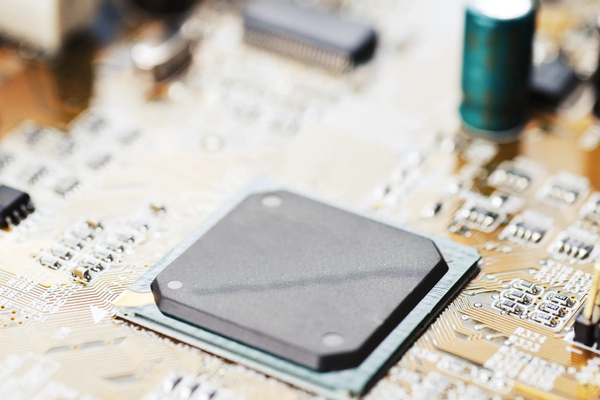
Laser marking is used to identify silicon wafers, but what are they? These wafers are a material that acts as a semiconductor, which is found inside all different types of electronic devices. It looks like a flat, circular disk with a mirrored surface.An essential characteristic of silicon wafers is that they have absolutely no impurities, so during the laser marking process, they need to be handled with extreme care and caution to keep them flawless.

Lasers are the perfect tool for when something needs to be perfectly precise, and in the case of the silicon wafer manufacturing process, precision is extremely critical. Here are some other characteristics of laser beams used during the marking process:

Annealing is the extremely efficient process of heating surfaces with a laser beam. Once the surface is heated, the oxygen below the surface is diffused (oxidation). After everything is cooled, you can see a change in color.There are a few different colors that can be produced from annealing, such as yellow, red, and green. These colors can be changed based on the temperature during the marking process. The temperature can go higher or lower based on three variables:
The lasers are extremely accurate and can make characters that are less than a millimeter tall. Due to how well this method words, annealing is very popular with laser marking silicon wafers.

The first step in marking silicon wafers is through computer interaction. During this stage of the process, a map of the wafer is viewed on a marking document. This is where the different parameters, functions, and other information is detailed. On the other side of the screen, a preview is available to see how the data will translate to the silicon wafer.After everything is set up correctly, the wafer will be placed inside the laser marking machine. A mechanical hand will take the wafer and bring it to the marking position. The whole process will be completely automated, with no human interaction necessary.Once the machine finds the target location, it will shine the laser onto the surface of the wafer. Once that is finished, it will transport the completed project to the receiving box where they can be taken away.

Using laser marking for wafer manufacturing is the perfect choice due to its precision. Its superior technology allows even the tiniest details always to be completely detailed and accurate. Markings on silicon wafers are often less than a millimeter tall and can be read by computers for easy tracking.
Not only is laser marking extremely precise, but the entire process is quick too. Entire stacks of silicon wafers can be laser marked in minutes, with each specific disk only taking a matter of seconds from placement, to marking, to completion. Laser annealing is slightly slower than some other marking methods, although it creates an amazing finish without removing anything from the surface.
When a silicon wafer is laser marked, nothing is actually stripped away from the surface. It simply causes a color change beneath the surface. Everything is kept in perfect condition.

The markings left on the silicon wafers are 100 percent permanent. Since the mark is left just below the surface by heat, there is no chance of it fading away.
The whole system is entirely automated. No human interaction is necessary. A mechanical arm is able to pick up single silicon wafers and transport them to the correct location inside the machine for marking. Once the laser has changed the surface color of the wafer, it will bring it outside of the machine.This makes laser marking machines completely safe to use since there will be no interaction with the lasers. Plus, the odds of costly mistakes will go way down. It takes away the variable of human error.
Laser marking does not use any type of chemicals or inks, which means it’s much safer for the environment than other marking methods. Lasers also don’t use much energy, making it an all-around great way to mark silicon wafers.

At Wafer World, we use the best available technology to provide you with the highest quality silicon wafers. Every step of the way, we put an incredible amount of care and precision into each wafer so that it is in perfect condition, free of any defects or issues.This comes right down to our automated laser marking machines, which allow us to mark the wafers without removing anything from the surface. If you are interested in purchasing our silicon wafers, we’d be happy to help you. Contact us today for inquiries!


