
Silicon wafers, the cornerstone of contemporary electronics, undergo a methodical evolution from raw materials to intricate semiconductor components. Understanding this progression is essential for comprehending the intricacies and significance of silicon wafer production. Let's illuminate the essential steps involved with silicon wafer manufacturers.
The process commences with the careful selection of high-purity silicon. This silicon is extracted from quartz and undergoes stringent purification to eliminate impurities.
The purified silicon is melted down and crystallized to form a cylindrical ingot. This process, often based on the Czochralski method, guarantees a singular crystal structure critical for semiconductor efficacy.
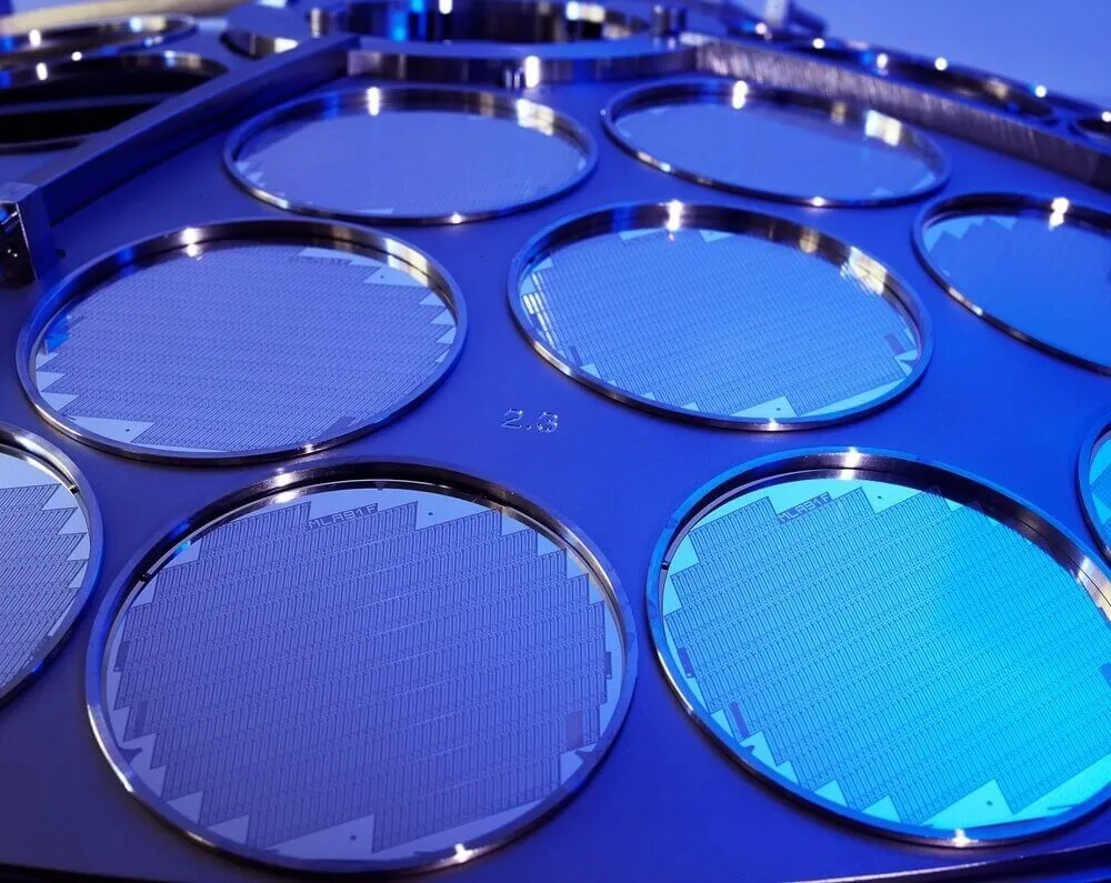
Upon reaching the desired diameter, the ingot is sliced into thin wafers using precise saws or wire-cutting techniques. These wafers, typically less than a millimeter thick, are the foundation for semiconductor fabrication.
Sliced wafers undergo mechanical and chemical polishing to achieve a flawless surface finish. This procedure is critical for achieving uniformity and improving the wafer's electrical characteristics.
To impart specific electrical characteristics, dopant atoms like boron or phosphorus are introduced into the silicon lattice through diffusion or ion implantation processes. This phase customizes the wafer's conductivity to meet diverse semiconductor needs.
A pivotal process in semiconductor production, photolithography entails masking and exposing the wafer to UV light through intricate patterns, defining the layout of circuitry. This stage is indispensable for creating precise features crucial for electronic components.
Chemical etching eliminates unwanted material, while deposition techniques add thin layers of materials like silicon dioxide or metal onto the wafer surface. These periods build the complex structures necessary for semiconductor functionality.
Annealing methods improve the electrical properties of the wafer while thorough testing maintains quality and performance. Wafer testing involves various electrical and visual inspections to identify defects and enhance reliability.

The process of creating Wafer World silicon wafers entails a symphony of precision, chemistry, and engineering expertise. Each step significantly shapes these diminutive yet indispensable components that power our digital realm.
Understanding this process offers insight into the bedrock of modern electronics and underscores the pivotal role of silicon wafer production in propelling technological advancement. Call us for more info!


