
If you're looking for substrates for semiconductor, MEMS, photonics, or advanced packaging applications, you've narrowed your options to SI wafers or fused silica wafers. Both are widely used, but they address very different engineering problems.
Choosing the wrong one can result in performance issues, process incompatibilities, or unnecessary costs.
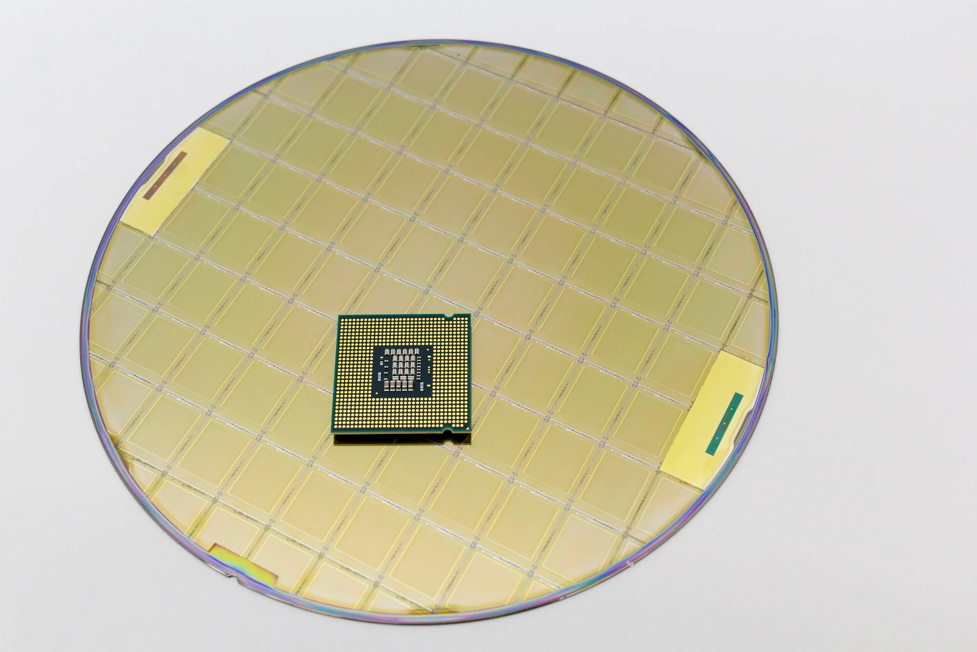
An SI wafer (Silicon wafer) is composed of crystalline silicon and serves as the foundation for the majority of semiconductor manufacturing. SI wafers can be conductive, semiconductive, or highly resistive, depending on their doping and resistivity.
Key characteristics of SI wafers include:
SI wafers are ideal when electrical performance, integration, and process compatibility are critical.
A fused silica wafer is composed of high-purity amorphous silicon dioxide (SiO₂). Unlike silicon, it is electrically insulating and optically transparent over a broad range of wavelengths.
The main characteristics of fused silica wafers are:
Fused silica wafers are chosen when optical clarity, insulation, or dimensional stability matter more than electronic functionality.
Silicon wafers and fused silica wafers can be very different. SI is conductive or semiconductive, supporting active devices. Meanwhile, fused silica is an insulating material, making it ideal for isolation and optical platforms.
While both have their key advantages, using them in the wrong situations can quickly damage your project.
There’s no universal “better” choice, only a better fit for your application. If you need help finding the right substrate, reach out to Wafer World for assistance.


