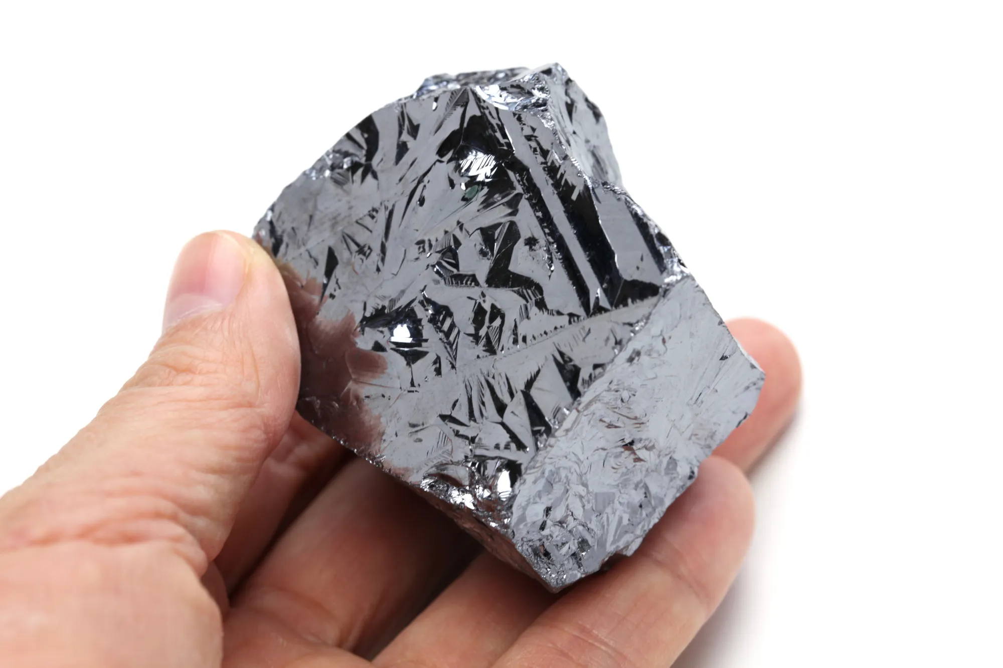
A highly pure and defect-free single crystal material is used to create a Si wafer. The extrinsic semiconductor produced in this process is used in several electrical devices. So, if you’re interested in extrinsic semiconductors, then read on to know more about the dopants in silicon that makes extrinsic semiconductors possible.
Si wafer doping is the process of changing an intrinsic semiconductor to an extrinsic semiconductor, through the introduction of impurities. Impurity atoms are atoms of a distinct element and they serve as either donors or acceptors to the intrinsic semiconductor. They manipulate or modify the electron and hole concentration of semiconductor.
Extrinsic semiconductors have two types, the n-type and the p-type. A negative-type extrinsic silicon semiconductor is a product of doping silicon with an n-type element. Most of the charge carriers are also electrons. While the positive-type extrinsic semiconductors are created through doping silicon with a p-type element from the group III A. And most of its charge carriers are holes because the dopants are acceptor atoms.
Common applications of extrinsic semiconductors are electrical devices. Examples are a semiconductor diode, transistors, bipolar junction transistors, NPN transistors, PNP transistors, and Field-effect transistors.

Whether you need a Si wafer, n-type semiconductor, or a p-type semiconductor, you can get it all at Wafer World. At Wafer World, our 20 years of experience in the industry has allowed us to master our craft-producing only the best wafers and providing excellent customer service to all our clients worldwide. Call us today for any inquiries or buy wafers online!


