Processors may only be big enough to fit the palm of your hand, but their capabilities are impressive. Despite their size, they can accommodate billions of tiny transistors. Their journey from being a Si wafer to a fully functional processor is equally fascinating. Below are the 10 steps involved in building a silicon processor for computers.
.jpg)
The silicon processors inside computers trace their origins from a mundane source – sand. However, chip makers use a specific type called silica sand. Silica sand is made up of about 95% silicon dioxide. SiO2 can also be found in regular sand. However, ordinary sand has only about 80% silicon dioxide content, less than how much semiconductor manufacturers need to make wafers and chips.
Once the sand arrives at the fabrication plant, factory personnel add carbon and heat the mixture in a furnace. The heating process bonds carbon with the sand’s oxygen content, creating carbon dioxide and freeing 99% pure silicon. Mixers remove the silicon to refine it further to produce electronic-grade silicon suitable for growing crystals.
Electronic-grade silicon is polycrystalline in nature. The points that join each crystal in the material mess up electronic signals and render chips defective. Thus, manufacturers must extract individual silicon crystals before making wafers and chips.
There are two processes for monocrystalline silicon from electronic-grade silicon.
The Czochralski method melts silicon crystals in a container attached to a spinning crucible. Once there is enough molten silicon, technicians drop a small ingot into the mixture. The molten silicon container is then rotated opposite the direction where the crucible is turning. The process draws out a silicon rod, which is then cut into wafers.
The float zone method eschews a quartz crucible and uses a feedstock infused with argon gas instead. The argon gas keeps the impure silicon crystal suspended in the air as it floats down through a molten area where it interacts with the silicon to create a monocrystalline ingot. The resulting crystal is pulled back up and extracted.
The growing process also includes the doping procedure, which introduces other elements to manipulate the conductivity of the silicon.
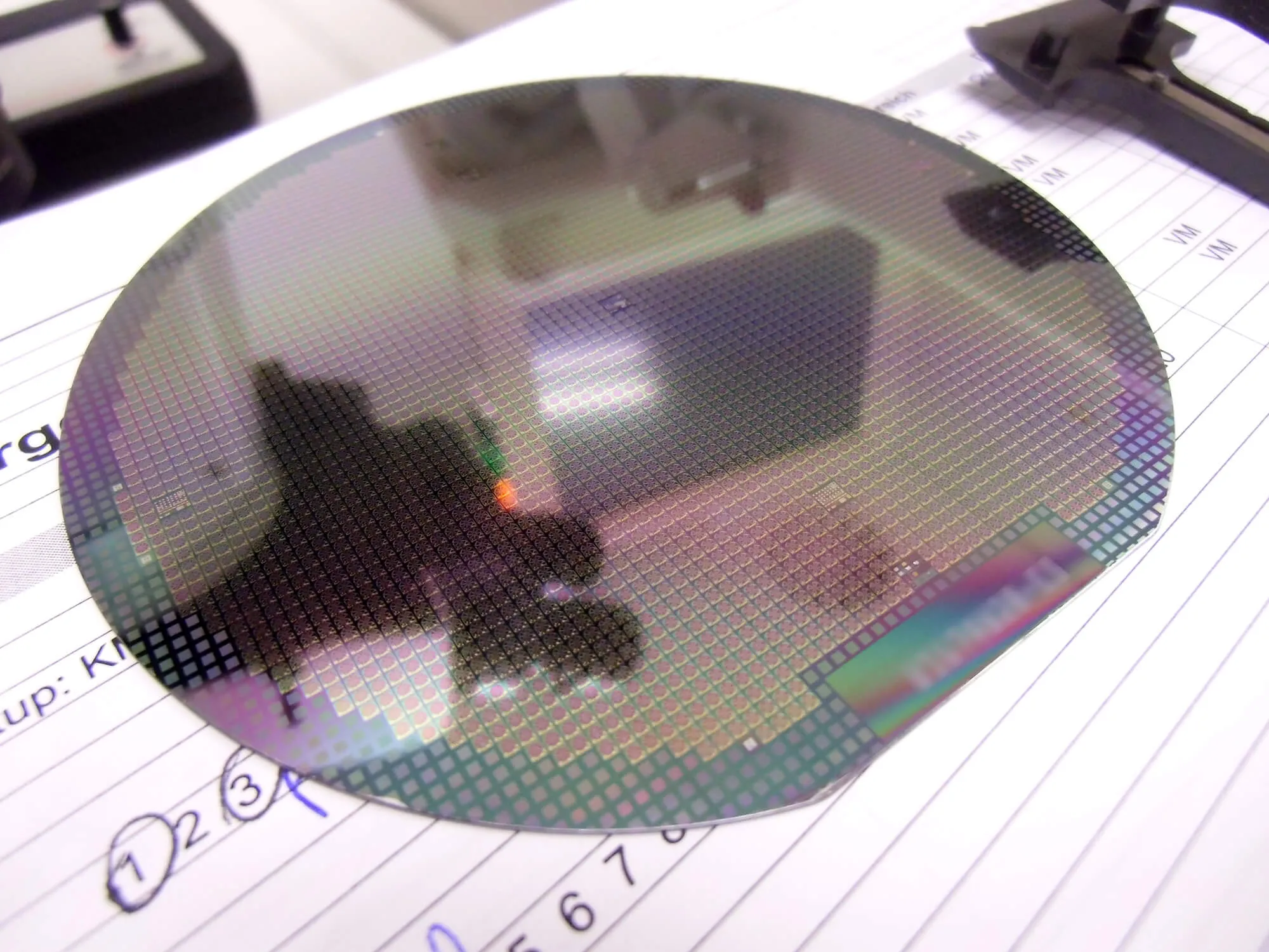
The boule, or the silicon rod created by the growth process, is taken to a cutting device and sliced into individual wafers. Each individual wafer is precisely cut to a thickness of 0.775 millimeters. This is the thinnest that wafers can go; any thinner and they will not survive the entire fabrication process.
The cutting gadget leaves wafers with sharp or rough edges. These edges are smoothed out while the surface goes through “lapping.” The lapping process results in a polished wafer, which is then exposed to nitric, hydrofluoric, and acetic acids to further burnish the surface.
Photolithography refers to the process of embedding circuit patterns to the surface of the wafer. This step is essential for guiding chip makers in assembling the components needed to create a working processor.
The process begins by coating the wafer with a photoresist, an ultraviolet-sensitive solution that hardens with light exposure. At the same time, the crew creates a stencil of the circuit pattern by burning the draft using ultraviolet light into a surface called the mask. Once the mask is ready, the manufacturers will apply it to the surface of the wafer and expose the mask again to UV light.
The exposure hardens the photoresist covered by the mask and embeds the circuit in the Si wafer. The remaining liquid photoresist is then chemically removed.
With the guide now in place, engineers can add the most important processor component – the transistor, which experts formally refer to as the Metal Oxide Semiconductor Field Effect Transistor or MOSFET.
MOSFETs act as switches for the electrical current that the chip receives. It requires the creation of n-type and p-type wells. The p-type well is made by exposing the wafer to boron ions, while the n-type well requires the same process but using phosphorous ions. The n-type well defines the switch and drain regions, which will need a second photoresist layer.
Logic gates control the functions of the MOSFETs. Theoretically, gates take an input, process it, and create an output. Engineers use logic gates to define how the chip functions. For example, gates help Random Access Memory chips to edit values processed by software.
Traditionally, transistors have only two gates. However, technological advancements have made three-dimensional gates now possible. Chips also combine multiple types of gates to perform their specified functions.

With the gates and switches in place, the next step would be to connect them with copper. The first step is to introduce silicon oxide to insulate the circuits. Afterwards, the makers add another layer of photoresist that identifies parts of the insulation that needs to be holed with hydrofluoric acid. They also add another photoresist to create the interconnecting tracks between the components.
The final step is to electroplate the circuits with copper. This also creates conductive connections between the switches and gates. All that remains is to clean off excess copper from the wafer.
After all the switches and gates are connected, it’s time for the manufacturer to close the circuit. This is vital to prevent shorts that could damage the dies or cause them to stop working. Multiple layers of metal on each MOSFET make sure all circuits are complete. At the same time, silicon oxide insulation keeps the tracks from crossing.
The quality control process ensures that there are no defective products shipped out to potential buyers. Customer satisfaction is a vital issue for chip makers, just like any other business, and quality assurance is their way of maintaining a positive reputation.
The processor QA routine involves visually checking the alignment of every component in the chip. There are various methods of optical inspection used for processor quality control. One of these is Terahertz imaging, which can output images with high spatial resolution and clarity.
A wafer probe also checks each individual die to identify non-functioning ones, which are discarded. Chips with tolerable defects may be retained and recycled for other products.

Finally, manufacturers encase the chip in a special package to keep it safe. Without this packaging, the chips can inadvertently get into contact with static electricity that can damage their contacts. The casing also keeps out the elements that corrode the chip’s metal parts and debris like dust. Last but not least, the case helps connect the semiconductor to the circuit board, like the motherboard.
Do You Need a Si Wafer Supplier?
Having a supplier with a reliable manufacturing process is vital. Our silicon wafers go through stringent quality control measures to ensure customer satisfaction. Call us now and learn more about our products.


