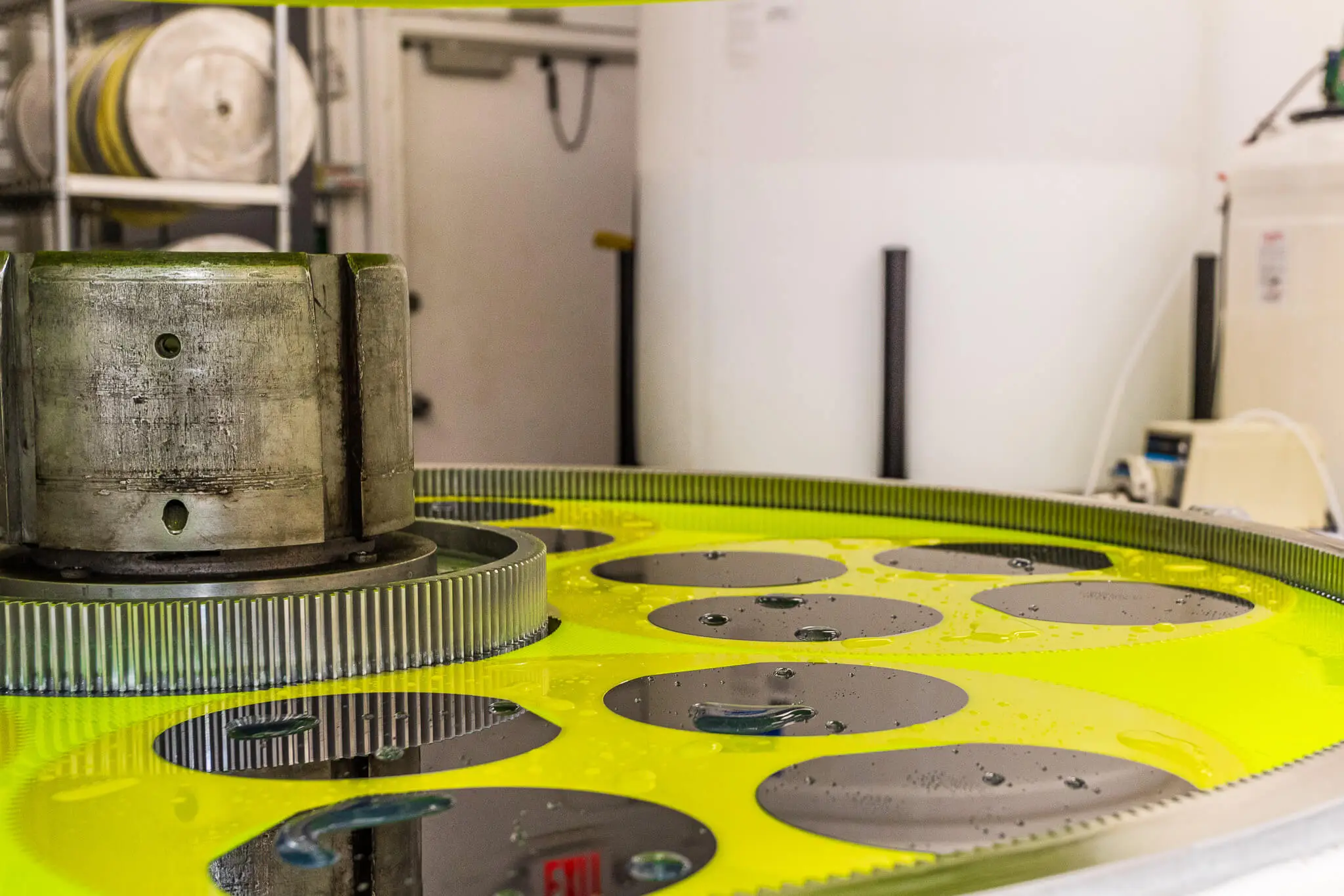
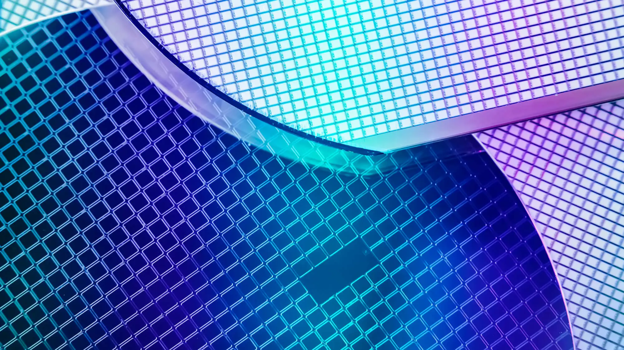
Every modern semiconductor device relies on one often-overlooked component: the dielectric. On a silicon wafer, dielectric materials influence how electric fields behave, how charges are isolated, and how well devices perform over time. Understanding that is crucial to optimizing manufacturing, yield, and long-term device reliability.
When exposed to an electric field, a dielectric acts as an electrical insulator and can store and control electric energy. Dielectrics are deposited or grown on silicon wafers in semiconductor manufacturing to separate conductive regions, form gate oxides, reduce leakage, and safeguard sensitive structures.
Silicon dioxide (SiO₂), silicon nitride (Si₃N₄), and advanced high-k materials are some examples of typical dielectric materials used in scaled devices.
While dielectric constant often gets the most attention, several properties matter in practice:
Optimizing these properties requires balancing electrical performance with manufacturability.
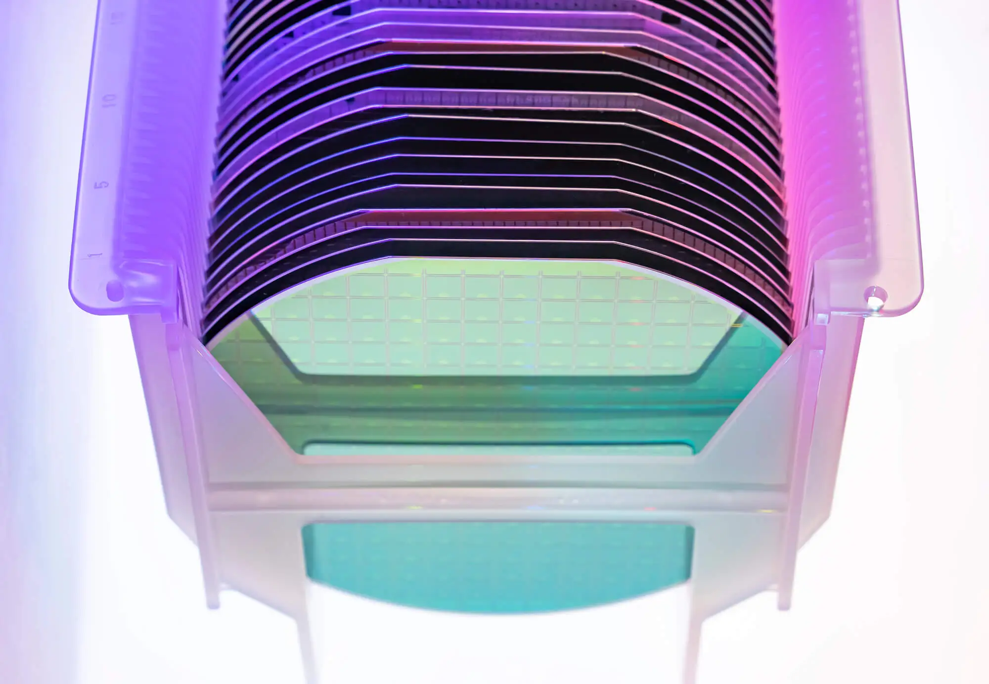
The dielectric performance cannot be separated from the silicon wafer. Crystal orientation, doping levels, surface roughness, and contamination influence dielectric growth and deposition.
Do you need a silicon wafer with specific qualities for your project? Contact Wafer World and let’s work together to help you achieve cleaner interfaces, more uniform films, and improved long-term reliability.


