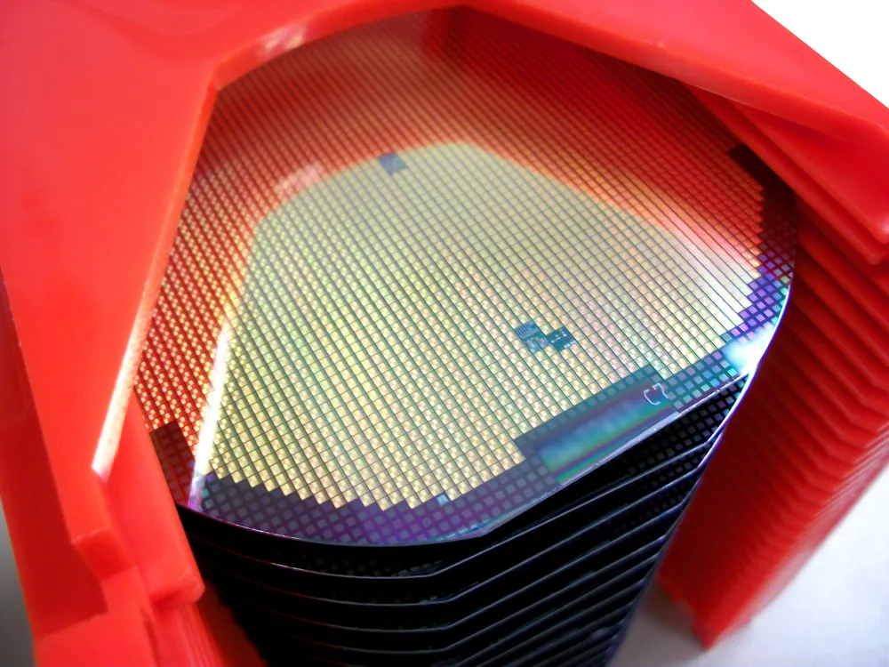
Silicon wafers are all around you at any given moment in time. They are in practically every form of technology that has been produced in the past twenty years and is only becoming more prevalent. Silicon wafers are an extremely useful component in electronic circuitry and if you plan on using them in a project, it’ll be important to know about the different types of wafers that are made from silicon wafer processing.
Doped silicon wafers are created by adding dopants into the silicon during the formation process. Adding boron into the mix will create a P-type material. Adding other elements like arsenic, phosphorous, or antimony will create an N-type material. P-type silicon wafers have several positively-charged holes while N-type silicon has a negatively-charged electron in it. The amount of dopant found in the wafer will determine if it is extrinsic or degenerate. If it is extrinsic, it has very little amounts of dopant. If it is degenerate, it has a higher concentration of dopants in it.
Unlike doped silicon wafers, undoped silicon wafers do not have any dopants in them. They are made up strictly of pure crystalline silicon. This form of silicon wafer is known as the ideal semiconductor. Undoped silicon wafers are also known as intrinsic silicon wafers.

Have you been looking for more information about silicon wafer processing? If so, contact us today. Wafer World is a verified vendor by the US Federal Contractor Registration and is here to help you find exactly what you are looking for.


