February 18, 2026
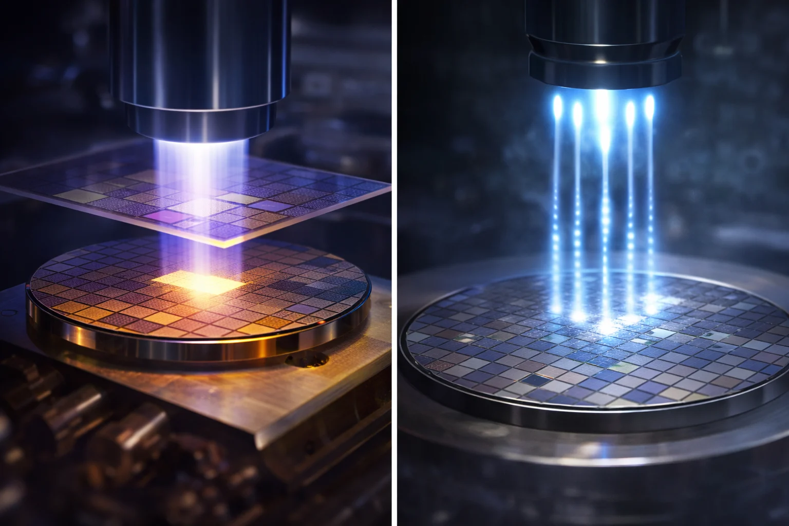
Shop NowModern semiconductor devices rely on precise silicon wafer processing to transform raw substrates into functional integrated circuits. From insulating layers to patterned features, each step in fabrication must be tightly controlled to ensure electrical performance, uniformity, and yield.
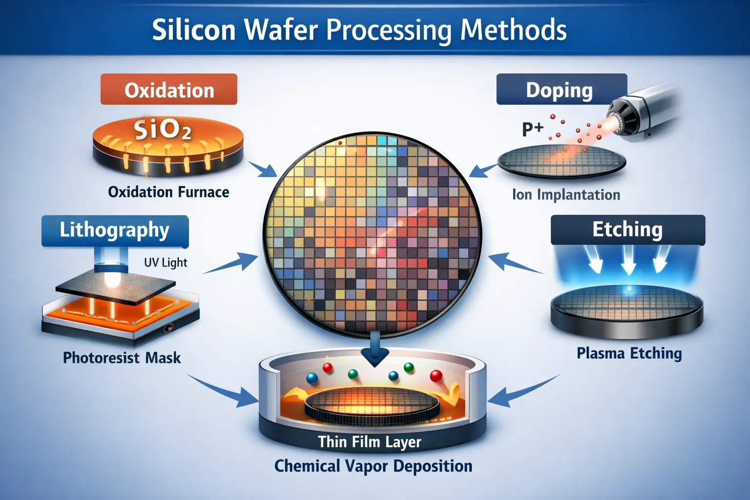
Four core methods define much of this workflow: oxidation, doping, lithography, and etching.
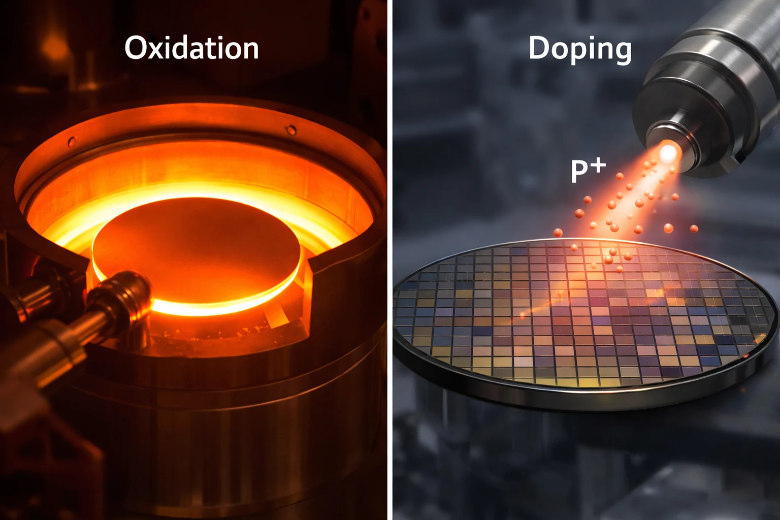
Thermal oxidation creates a thin layer of silicon dioxide on the wafer surface. This oxide layer serves as an insulator, gate dielectric, or protective barrier during later fabrication steps.
Thickness control is critical, as variations directly influence capacitance and device scaling. High-temperature furnaces and clean environments help maintain consistent oxide growth across the wafer.
Doping modifies the electrical properties of silicon by introducing controlled impurities such as boron or phosphorus. Through ion implantation or diffusion, manufacturers adjust carrier concentration and conductivity.
Precise dose and energy settings ensure accurate junction depth and minimal crystal damage. Careful annealing follows implantation to activate dopants and restore lattice structure.
Photolithography defines circuit patterns by transferring geometric designs onto the wafer surface. A light-sensitive photoresist is applied, exposed through a mask, and developed to reveal specific regions for processing.
As feature sizes shrink, alignment accuracy and resolution become increasingly important. Advanced tools help maintain pattern fidelity across high-volume production.
Etching selectively removes material to form trenches, vias, and circuit pathways. Wet etching uses chemical solutions, while dry etching relies on plasma processes for greater precision and anisotropy. Uniform etch rates and controlled selectivity prevent damage to underlying layers.
Each of these methods plays an essential role in silicon wafer processing, working together to build complex semiconductor devices layer by layer. At Wafer World, we support research and production needs with high-quality substrates and tailored wafer solutions.
To learn more about specifications or discuss your project requirements, contact us today and connect with our team.


