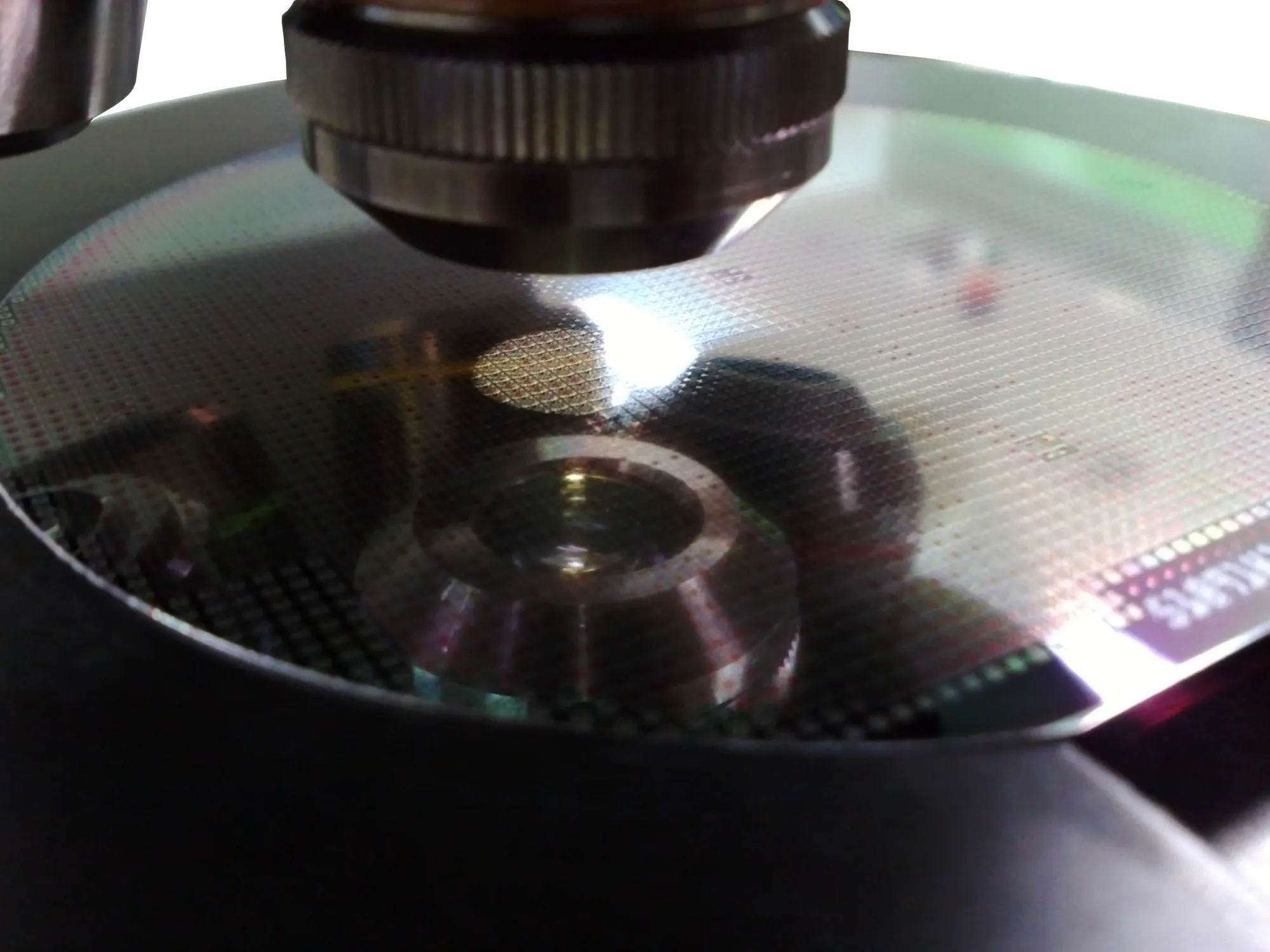
Silicon wafers are the building blocks of integrated circuits and semiconductors, which are the key components found in our everyday electronic devices. If you’re wondering how they’re made, here is how silicon wafer processing is done:
Wafers begin with a single crystal silicon ingots that are grown using either the CZ method or float zone method. The ingot is then sliced into a specific length and diameter. A notch or an orientation flat will be introduced to a part of the peripheral to know the crystal orientation.
Using a diamond inner peripheral blade, wafers are sliced one by one from the ingot-for small diameter wafer processing. For large diameter wafers, blocks are sliced at the same time with a wire-saw.
Wafers are lapped on both sides using a rotating lapping plate. This is to get rid of the damaged surface layer and to reach the desired thickness. Etching is a method used to completely remove the damaged surface, using either physical or chemical etching.
In order to eliminate thermal donors, the wafer needs to go through donor annihilation heat treatment. This will help restore the predetermined specific resistance.

The intricate processes involved in silicon wafer processing is done to make sure that the wafers produced are of premium quality. If you’re looking for any type of wafers, you can get quality wafers from Wafer World. Our 20 years of experience in the industry has allowed us to provide all our clients' excellent wafers and quality customer service. Call us today for inquiries or buy wafers online!


