In the field of semiconductor manufacturing, silicon wafer processing stands as a crucial element, facilitating the creation of intricate electronic devices that power our modern world. However, this journey from raw silicon to functional chips is fraught with obstacles, demanding constant innovation to overcome hurdles and push the boundaries of what's achievable.
As semiconductor technology advances, the demand for smaller, more powerful chips escalates. Yet, this quest for miniaturization poses challenges in maintaining yield and quality while stretching the limits of lithography and material science.
Seamlessly integrating various fabrication steps is critical for efficiency and cost-effectiveness. However, achieving this integration without compromising performance remains a significant challenge, particularly as the number of processes increases.
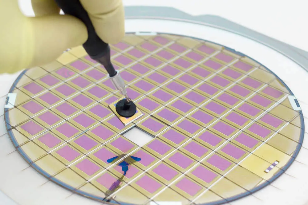
Warranting high yields is paramount in semiconductor manufacturing to maximize profitability. However, defects and variations in the silicon wafers can significantly impact yield, necessitating innovative solutions to detect and mitigate these issues.
The semiconductor industry operates on narrow margins, necessitating continuous efforts to reduce production costs without sacrificing quality or performance.
Manufacturers can use machine learning and artificial intelligence algorithms to analyze vast amounts of data in real-time to optimize process parameters and enhance yield.
Multi-patterning techniques like self-aligned double patterning (SADP) and self-aligned quadruple patterning (SAQP) have been developed to overcome the limitations of traditional optical lithography. This enables the creation of smaller feature sizes with improved resolution.
Exploring alternative materials such as III-V compounds and transition metal dichalcogenides (TMDs) opens new avenues for semiconductor devices, offering higher performance and efficiency compared to traditional silicon-based technologies.
By stacking multiple layers of transistors vertically, 3D integration allows for increased device density and improved performance while reducing interconnect lengths, addressing some of the challenges associated with scaling down to smaller feature sizes.
Wafer-level packaging techniques integrate packaging processes directly into the semiconductor manufacturing flow, reducing costs and improving device reliability by eliminating the need for traditional packaging methods.
While silicon wafer processing presents numerous challenges, ongoing innovations in process integration, yield enhancement techniques, and materials science continue to propel Wafer World forward, enabling the development of increasingly advanced and powerful electronic devices. Call us today to order!


