Permittivity and dielectric constants are often treated as abstract material properties; however, in silicon-based devices, they directly affect signal speed, power efficiency, leakage, breakdown behavior, and long-term reliability. Engineers, researchers, silicon wafer suppliers, and procurement teams working with advanced semiconductor devices must understand how these properties behave in silicon in order to make informed design and sourcing decisions.
This guide explains the physics of permittivity in silicon, how it varies across materials like SiO₂ and Si₃N₄, and why dielectric control is important when selecting the right providers.

Permittivity (ε) describes how a material responds to an electric field by polarizing and storing electrical energy. It determines how electric fields propagate through a medium and how much charge can be stored per unit of voltage.
The dielectric constant (κ or εᵣ) is the relative permittivity of a material compared to vacuum:
In practical semiconductor engineering, the dielectric constant is what designers use to predict capacitance, coupling effects, and field strength inside devices.
At room temperature and low frequencies, crystalline silicon has a dielectric constant of ~11.7. This relatively high value plays a critical role in:
Because silicon is not just a passive mechanical substrate but an electrically active medium, its dielectric behavior affects switching speed, leakage current, and breakdown voltage.
A common misconception is that materials with higher dielectric constants are more conductive. In reality, the dielectric constant describes polarization, not charge transport. This means conductivity depends on free charge carriers.
Silicon can behave as:
This duality is why dielectric properties must be carefully controlled during wafer manufacturing—especially for RF, power, and mixed-signal applications.
Besides the aforementioned, the key factors that influence silicon’s dielectric properties include:
Heavy doping alters carrier concentration, which can modify effective permittivity, especially at low frequencies. This occurs because free carriers contribute to space-charge polarization, increasing dielectric response but also introducing frequency-dependent dispersion and higher dielectric losses.
At higher frequencies, polarization mechanisms lag behind the applied field, reducing the effective dielectric constant. Only faster electronic polarization can respond at GHz and above, while slower dipolar and space-charge effects become negligible, lowering the material’s apparent permittivity.
Permittivity slightly increases with temperature due to enhanced lattice vibrations. As thermal energy rises, increased atomic displacement enhances polarizability, although excessive temperatures can introduce instability and leakage in semiconductor devices.
Defects, dislocations, and oxygen content influence local electric fields and polarization behavior. These factors highlight why wafer-level processing is critical—and why not all silicon wafers behave identically.
Silicon dioxide remains the most widely used dielectric in semiconductor fabrication.
With a dielectric constant: ~3.9, SiO₂ is foundational in gate oxides, field isolation, and surface passivation. Some of the key advantages this material offers are:
For all these reasons, despite the rise of high-κ dielectrics, SiO₂ remains critical for interface engineering.
Silicon nitride has a dielectric constant of ~7.0–7.5, making it useful when higher capacitance is needed without extreme scaling. This is the case for uses such as:
However, one downside of Si₃N₄ is that it introduces a higher fixed charge density, making process optimization and substrate quality essential.
As device scaling pushed SiO₂ to atomic thicknesses, leakage became a limiting factor. This led to the adoption of high-κ materials such as:
These materials increase capacitance without reducing physical thickness—but they still rely on silicon substrates with tightly controlled dielectric properties to perform reliably.

Many manufacturers focus on thin films, but substrate permittivity sets the baseline for everything built on top. When you have high-quality silicon wafers as a base, you can achieve:
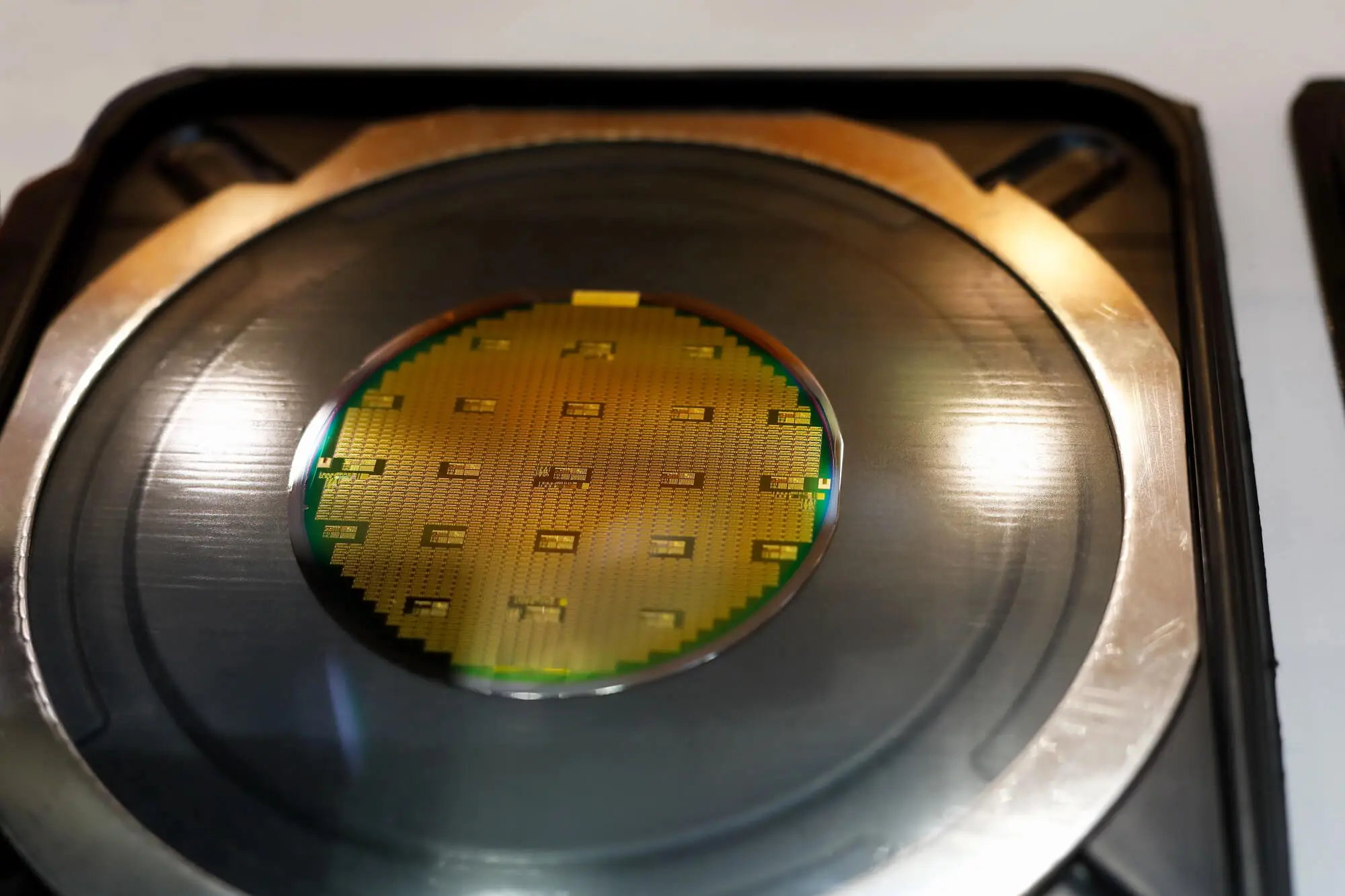
All of these factors are especially critical in applications such as power electronics, RF and mmWave devices, and advanced logic and memory, among others. For that reason, choosing experienced silicon wafer suppliers ensures dielectric consistency that downstream processing alone cannot fix.
Dielectric properties of silicon directly impact:
As devices become more complex, dielectric optimization becomes a competitive advantage—not just a material parameter.
When dielectric performance matters, leading silicon wafer suppliers focus on:
These factors ensure that permittivity and dielectric behavior remain stable across batches—reducing risk in high-value device fabrication.
Do you have any remaining questions about permittivity and dielectric constants in silicon? Here are some FAQs we get from our clients—with their answers.
Yes. Effective permittivity decreases at higher frequencies due to polarization lag.
No. Permittivity describes polarization; dielectric strength describes breakdown voltage.
Interface quality, reliability, and thermal stability still favor silicon-based systems.
Permittivity and dielectric constant are more than just theoretical concepts; they are design constraints, yield drivers, and sourcing criteria. Understanding how these properties behave in silicon enables engineers and buyers to make informed decisions throughout the semiconductor value chain.
Whether you're optimizing device performance or evaluating silicon wafer suppliers, dielectric knowledge is crucial. Do you need some help finding the right materials for your project? Contact Wafer World for a personalized quote!


