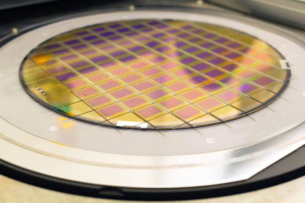
Often recognized for their role in semiconductor manufacturing, ultra flat wafers possess an array of lesser-known applications that highlight their adaptability and versatility. Here, we explore several unconventional uses of these wafers, showcasing their potential beyond traditional boundaries.
Ultra flat wafers form the backbone of photovoltaic cells, essential components of solar panels. Their exceptional flatness and purity enhance the efficiency and lifespan of solar energy systems, enabling the harnessing of sunlight for sustainable electricity production.
In the realm of microfluidic devices, ultra flat wafers play a crucial role in enabling precise manipulation and control of fluids on a tiny scale. These devices find applications in diverse fields, including biomedical research and chemical analysis, facilitating tasks such as drug delivery and lab-on-a-chip technologies.
Leveraging their optical properties, ultra flat wafers are used to produce high-quality lenses for cameras, telescopes, and microscopes. Their uniform thickness and low defect density contribute to superior image resolution and clarity.
Micro-electromechanical systems (MEMS) sensors rely on ultra flat wafers to construct miniature mechanical structures integrated with electronic components. These sensors are employed in various industries, from automotive to aerospace, for applications such as motion detection and environmental monitoring.
Ultra flat wafers serve as templates for microfabrication processes, including lithography and etching, in the production of MEMS, microfluidic devices, and integrated circuits. Their precise surface characteristics facilitate the replication of intricate patterns with high fidelity.
In scientific research, ultra flat wafers serve as substrates for atomic force microscopy (AFM), enabling the visualization and analysis of surfaces at the nanometer scale. Their exceptional flatness and stability contribute to accurate topographical mapping of materials.
Ultra flat wafers are integral to the fabrication of thin-film transistors (TFTs), essential components in LCDs, OLED screens, and flexible electronics. These transistors enable precise control of pixel switching, resulting in vibrant and responsive display technologies.

The diverse applications of ultra flat wafers extend far beyond their conventional use in semiconductor manufacturing. From renewable energy to advanced sensing systems, these wafers continue to push the boundaries of innovation and discovery.
With Wafer World, you are sure to receive high-quality wafers! Call us to order!


