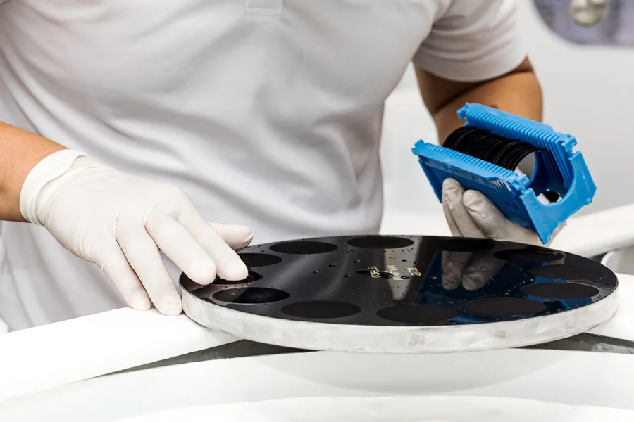
A single skipped step in silicon wafer processing rarely shows up right away. It shows up three months later, when a chip fails in the field, and an engineering team spends weeks tracing the defect back to a substrate that was never fully qualified. That gap between the shortcut and the consequence is exactly why so many buyers underestimate what this work actually requires.
For a broader look at how these issues surface across the industry, our news page tracks developments worth watching.
Most explanations of wafer processing stop at "slice, polish, ship." That description is technically true and practically useless. It tells a procurement manager nothing about why one batch performs flawlessly for five years while another introduces intermittent failures that never quite get diagnosed.
Silicon starts as a cylindrical ingot grown by the Czochralski method, in which a seed crystal is rotated inside a crucible of molten silicon until it pulls up a long, purified column of crystalline material. That ingot then gets sliced into individual wafers, and this is where the real work begins.
Each slice needs to be shaped, cleaned, and measured against tolerances that are often smaller than a fraction of a human hair. Wafer World's own silicon reclaim and fabrication services walk through this in more depth. Still, the short version is that raw slicing produces a rough, uneven surface that cannot go anywhere near a fab floor without further work.
Silicon wafer processing is a sequence, not a single action, and each stage exists because skipping any one creates a specific, predictable failure mode later on.
Miss one of these, or rush it to hit a shipping deadline, and the wafer might still look acceptable under a basic visual check. It will not perform acceptably once it reaches a customer's fab.
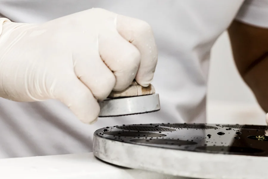
Here is a figure that rarely appears in general explanations of this process: a properly processed silicon wafer requires a total thickness variation (TTV) of less than 1 micron across its surface. Resistivity specs for Czochralski-grown wafers typically range from 0.001 to 100 ohm-cm. In comparison, float-zone wafers range from 100 to 10,000 ohm-cm, depending on the intended application. These are not arbitrary numbers. They are the difference between a wafer that supports a stable integrated circuit and one that introduces electrical noise that no downstream fix can correct.
The National Institute of Standards and Technology has spent years refining how these tolerances get measured. Its researchers developed an infrared interferometer capable of detecting thickness differences across a 300 mm wafer with a repeatability of just 5 nanometers, a level of precision that helps the semiconductor industry meet increasingly demanding quality-control benchmarks.
Related NIST research on wafer flatness shows that allowable flatness for 300 mm wafers was expected to drop to under 25 nanometers by 2015, a benchmark that pushed both polishing and metrology methods to their limits. That kind of measurement standard exists because even nanometer-scale inconsistencies compound as devices shrink and circuits get denser.
The consequences rarely stay contained to a single wafer. A batch with an inconsistent doping concentration can pass an initial visual inspection and still cause yield loss during photolithography, since uneven conductivity throws off exposure calibration across the whole lot. A wafer with excessive surface roughness from an incomplete polish step can cause adhesion problems during subsequent bonding or packaging stages.
These failures are also expensive in ways that go beyond the cost of the wafer itself. Rework, scrapped production runs, and delayed shipments ripple through a supply chain that is already under strain. The U.S. Department of Energy's supply chain assessment noted that current global silicon production struggles to keep pace with rising demand, leaving less room than ever for processing errors that can force a buyer back to square one.
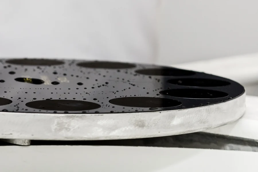
This is why the choice of who processes your wafers matters as much as the specification sheet itself. A supplier with decades of hands-on experience and a documented history of consistent quality control, like the team behind Wafer World's silicon and semiconductor wafer services, builds each stage around repeatability rather than speed alone.
It also helps to work with a company that controls conditions after processing is complete. Improper storage or handling can undo weeks of precise work, which is one reason clean room packaging exists as a dedicated service rather than an afterthought. Buyers evaluating a new supplier can browse the full product catalog or review a company's background through pages like Wafer World's company history before committing to a purchase order.
It is the full sequence of steps, including slicing, lapping, etching, polishing, doping, and deposition, that transform a raw silicon ingot into a finished wafer ready for semiconductor fabrication.
Timelines vary depending on wafer diameter, specification complexity, and order volume, but a full sequence from raw ingot to finished, inspected wafer typically takes several days to a few weeks.
Yes. Reclaiming involves stripping films and reconditioning the surface of used wafers so they can be reused, which is often more cost-effective than starting from a new ingot for testing or lower-tolerance applications.
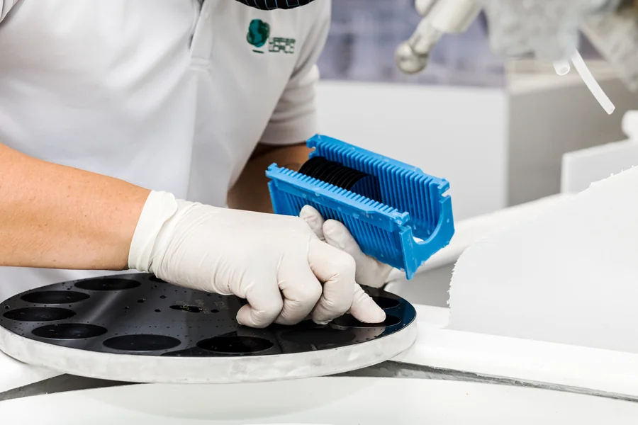
Skipping a step in silicon wafer processing might save a day on paper. Still, it tends to cost far more once a defective batch reaches production. If you need wafers processed to exact tolerances by a team that treats precision as non-negotiable, contact Wafer World and schedule a consultation to discuss your specifications before your next order goes out.




