
In advanced semiconductor manufacturing, ultra flat wafers play a critical role in enabling tighter geometries, improved lithography alignment, and consistent thin-film deposition for both MEMS and power devices.
Wafer flatness directly affects the depth of focus during photolithography. Even slight topographical variation can introduce overlay errors, impacting yield and device reliability.
Parameters such as total thickness variation and site flatness are key indicators of process control.
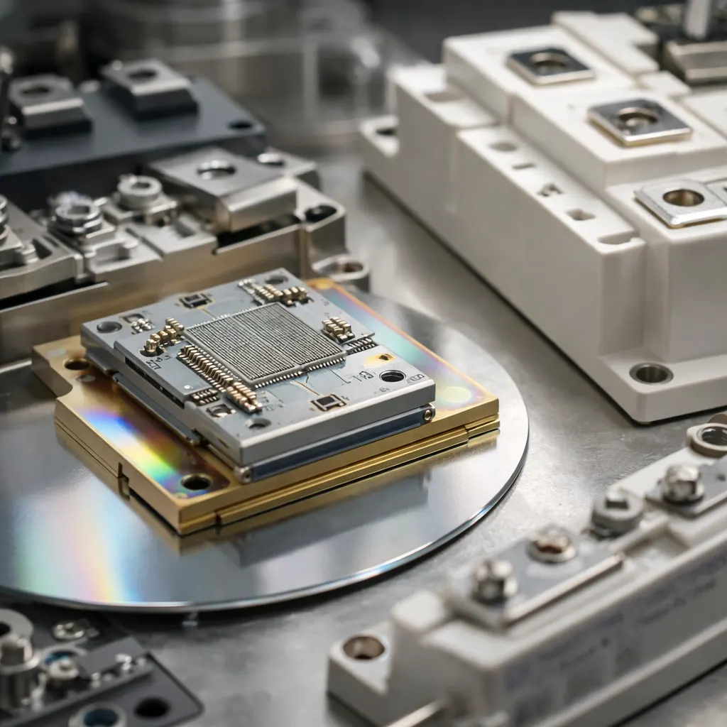
For MEMS devices, which often involve suspended structures and micromachined cavities, surface planarity is essential for accurate etching and layer stacking. In power electronics, particularly high-voltage and high-current devices, uniform substrates contribute to predictable electrical behavior and thermal distribution.
Advanced MEMS sensors depend on fine features and multilayer alignment. Ultra flat wafers help maintain consistent focal planes across the wafer surface, reducing pattern distortion.
Uniform surfaces support controlled plasma etching and even thin-film growth, which are essential in capacitive sensors, accelerometers, and RF MEMS components.
Power devices such as MOSFETs and IGBTs require tight dimensional tolerances. Substrate uniformity contributes to reduced leakage and improved breakdown characteristics.
Flat substrates promote even metallization and bonding, supporting efficient heat dissipation in demanding operating environments.

When fabrication tolerances tighten, material consistency becomes even more important. Ultra flat wafers support advanced manufacturing by reducing variability at every stage of processing.
At Wafer World, we provide precision-engineered wafer solutions backed by decades of semiconductor material expertise. If you are evaluating ultra flat wafers for MEMS or power electronics applications, contact us to discuss your technical requirements and get a quote.


