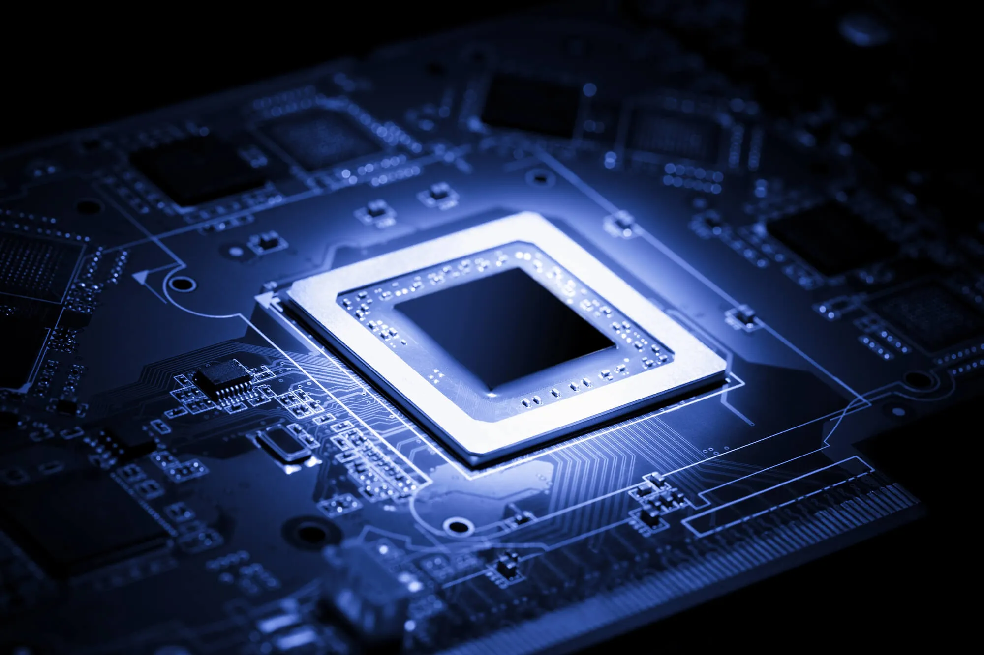
Accuracy in silicon wafer processing is more important than ever as the need for devices that are faster, smaller, and use less energy grows. Atomic Layer Deposition (ALD), a thin-film deposition technique renowned for its atomic-level control over film thickness, composition, and uniformity, is one of the most sophisticated methods making this precision possible.
Atomic Layer Deposition (ALD) is a vapor-phase technique for depositing ultra-thin films on a substrate, such as a silicon wafer. ALD uses self-limiting chemical reactions to create materials one atomic layer at a time, in contrast to conventional deposition techniques like Chemical Vapor Deposition (CVD) or Physical Vapor Deposition (PVD).
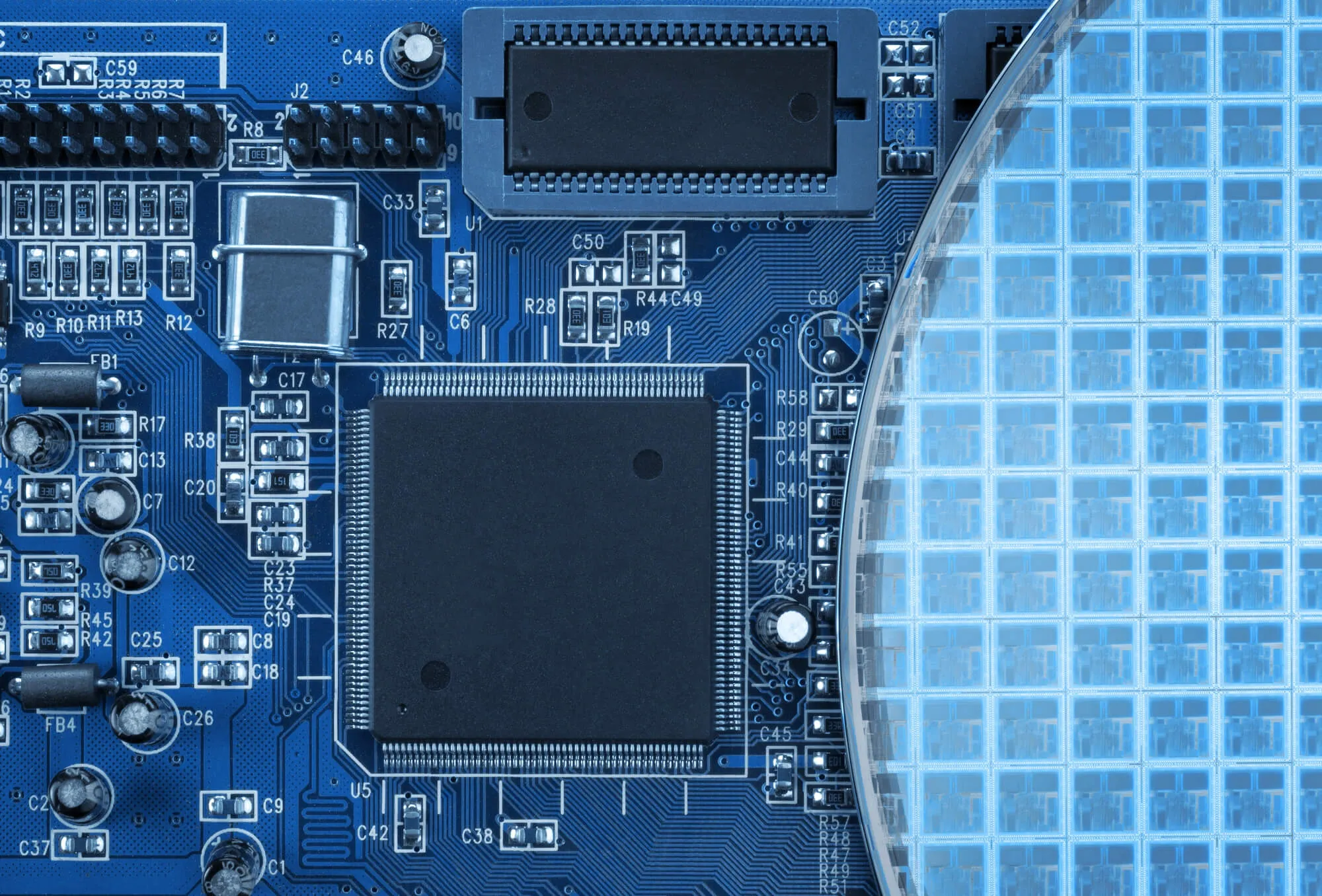
This process makes ALD ideal for applications requiring conformal coatings, even on ultra-thin substrates, which is crucial for modern transistors, memory devices, and advanced packaging.
ALD is essential for next-generation semiconductor device fabrication, offering key advantages like:
Atomic Layer Deposition is revolutionizing silicon wafer processing in the semiconductor industry. It is a fundamental technology for creating the most cutting-edge electronic devices of today due to its precision, consistency, and adaptability.
Understanding and utilizing ALD is essential to pushing the limits of contemporary semiconductor performance. Would you like to learn more about the wafer manufacturing process? Contact Wafer World today!


