Si wafers are extremely pure and very thin slices of crystalline silicon. Due to their affordability and conductivity, silicon wafers serve as a substrate for microelectronic devices and are particularly helpful when constructing electronic circuits. It's also at the top of the list regarding semiconductor usage, which has led to its widespread use in the technological and electronic industries among silicon wafer suppliers.
Despite their metallic appearance, silicon crystals are not fully composed of metals. Metals are effective electrical conductors because "free electrons" can move freely between atoms, and electricity is the movement of electrons. To learn more about this element, here's everything you need to know about silicon wafers.
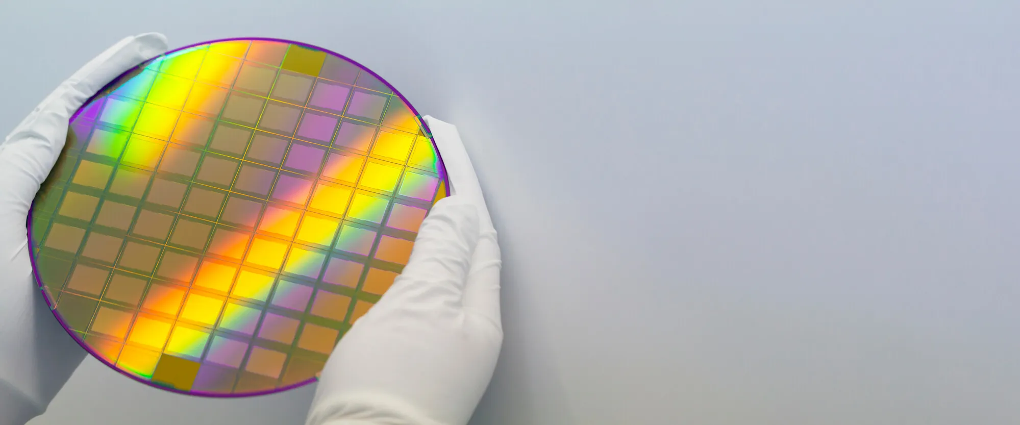
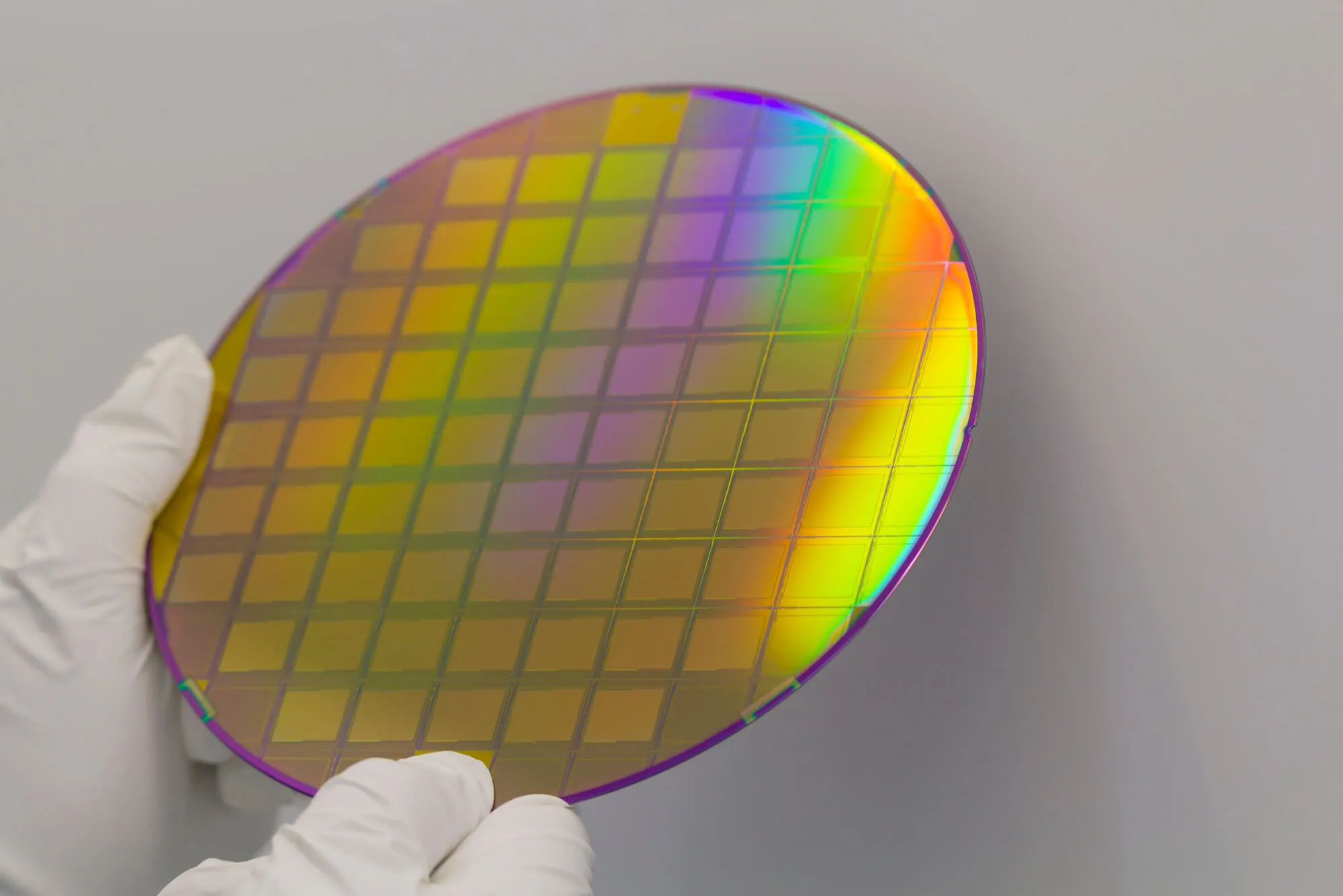
Several silicon wafers range in diameter from 300 mm (11.8 inches) to 25.4 mm (1 inch). The semiconductor manufacturing facilities, or fabs, are identified by the diameter of the wafer. The wafers selected are those that the fabs are intended to manufacture.
With the existing state-of-the-art fab using 300 mm, there is a progressive growth in the diameter, and with it is a suggestion to adopt 450 mm, to reduce the cost and improve throughput. Despite significant difficulties, Samsung, TSMC, and Intel were each doing independent research to introduce 450 mm "prototype" (research) fabs.
If you work in science or information technology, you must be familiar with silicon wafers. A gadget of this kind is widely used in physics, IT, and chemistry. Technically speaking, this tool is a thin, circular disc used to produce semiconductors and integrated circuits. The varieties used in electronics are silicon on insulator (SOI) and gallium arsenide, both of which require extremely precise manufacturing to provide high levels of efficiency. The growth of silicon wafers is handled with tremendous caution, even by seasoned professionals, and it is performed in a highly controlled environment.
These little wafers are doing big jobs. Many manufacturers use it to create computer chips. These are present in every electrical device, if not all of them. The composition contains a wide range of items before manufacture is finished. After being treated with care, they are packaged for delivery. The wafers are cleaned with a unique substance to ensure that the consistency of the wafers is not altered in any manner.
This substance, a mild acid, is utilized to remove contaminants and problems that arose during the sawing process. The price of a small factory and the equipment used to produce these parts are equal. Due to its role in electricity, silicon is the most common composite, but other materials are also included.
Without realizing it, we frequently see these little gadgets in advertisements for processors, computer chips, and microchips. Although consumers only consider the finished result and not the building block, silicon wafers are the most prevalent and significant construction element in any of your electrical gadgets.
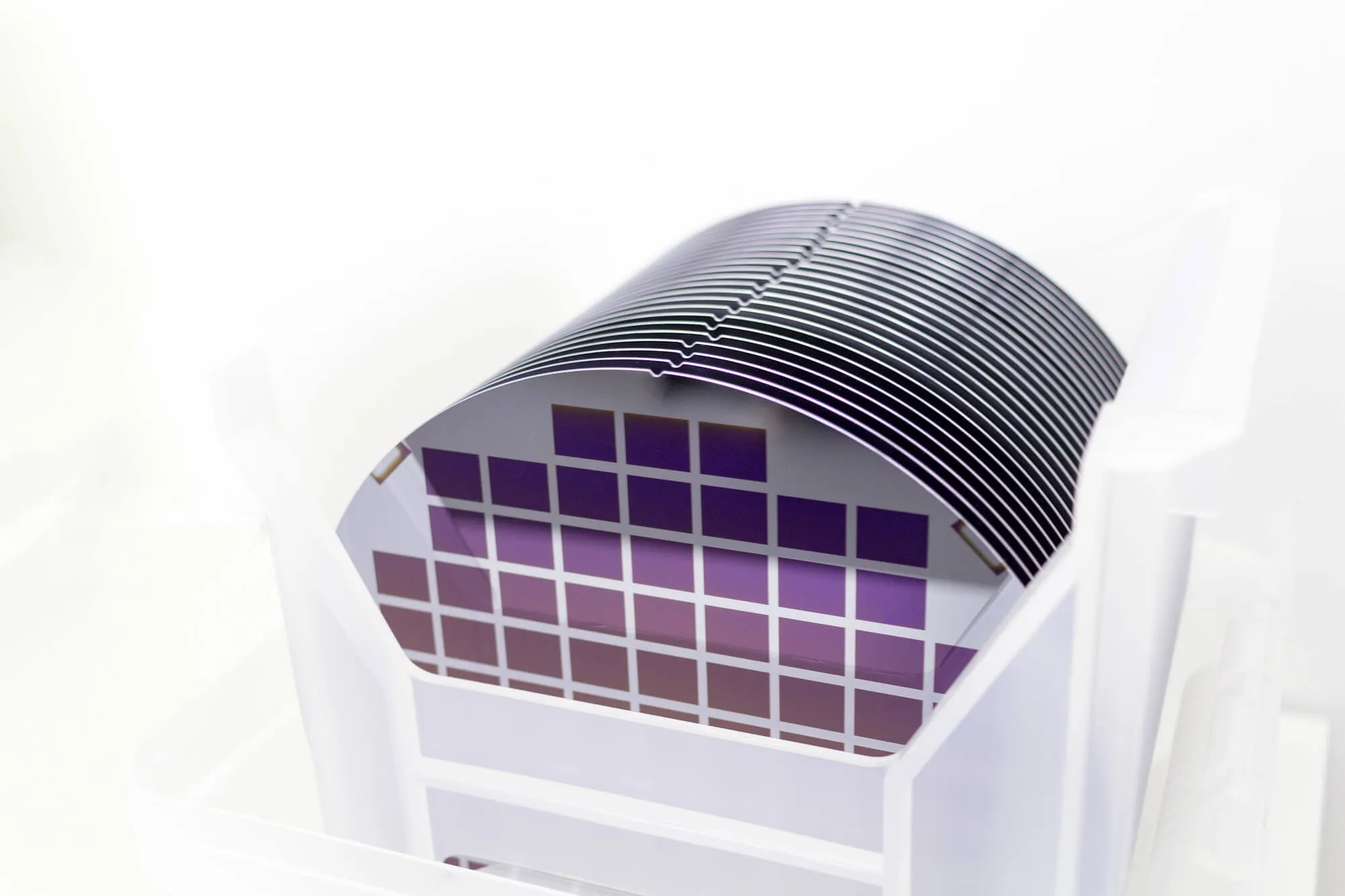
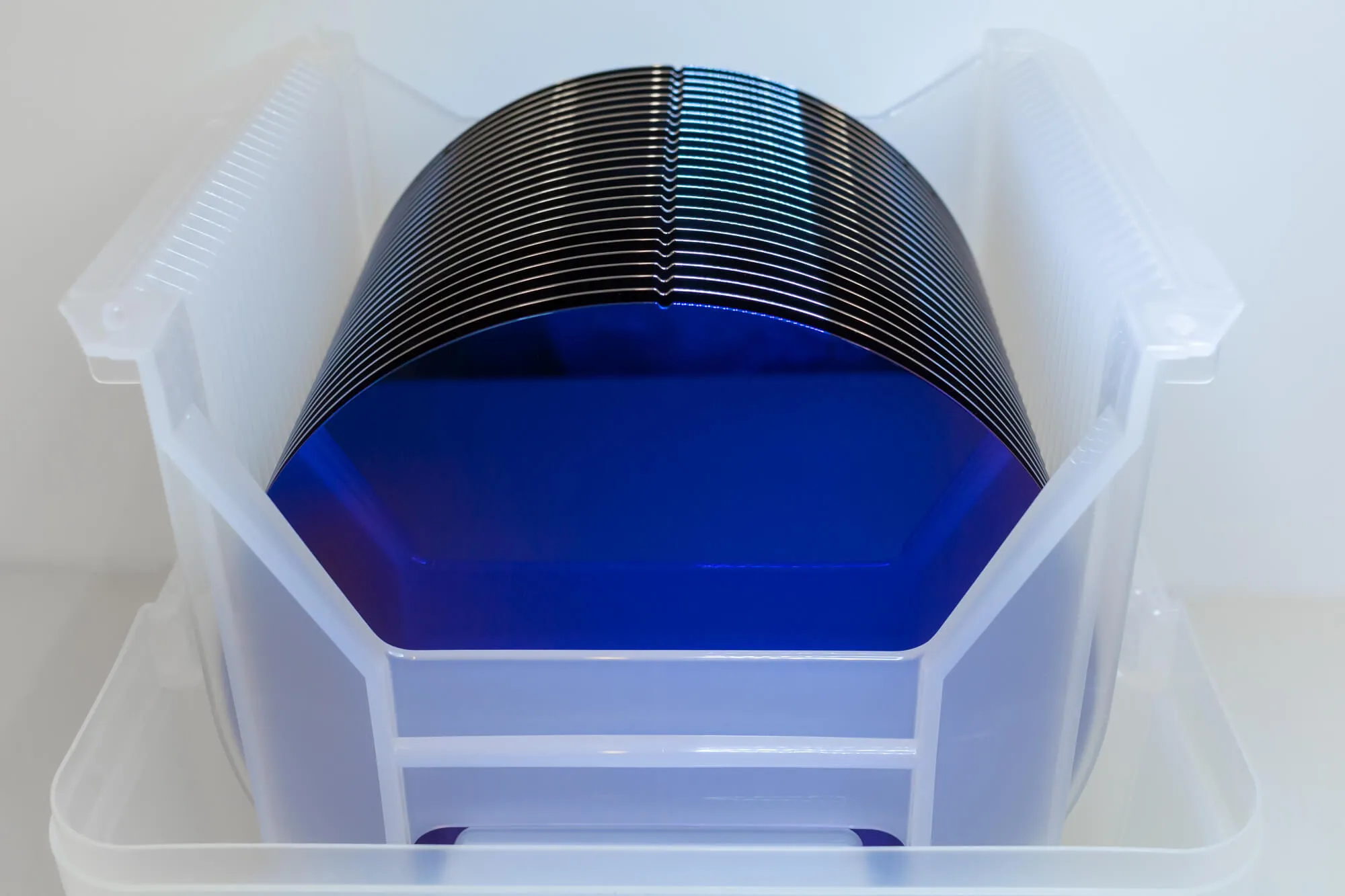
Silicon wafer is a thin semiconductor material used in electrical devices and integrated circuits. This material is a key component in many everyday devices, including computers, TVs, mobile phones, etc. There are various sorts of wafers, and each has unique characteristics. One should be familiar with the wide varieties of silicon wafers and their applicability to choose the best silicon wafer for a given project.
A silicon wafer that has been specially polished on both sides to create a mirror surface. This wafer is the greatest because of its superior qualities, such as purity and flatness.
They go by the name intrinsic silicon wafers as well. Such a semiconductor is silicon in its pure crystalline form, devoid of dopants over the entire wafer, making it the ideal and best semiconductor.
The two varieties of doped silicon wafers are N-type and P-type. The N-type doped silicon wafers are capable of holding either arsenic or phosphorus. In general, it is used to produce sophisticated CMOS devices. The P-type silicon wafer is doped with boron. It is mostly used for lithography or to create printed circuit boards.
Traditional wafers used to achieve surface integrity are called epitaxial wafers. There are two types of epitaxial wafers: thick and thin. Epi wafers with multiple layers and thick epitaxial wafers control the electric power and the device's energy consumption. Thin Epitaxial Wafers are frequently used in special MOS equipment.
These wafers are used to electrically isolate the monocrystalline silicon's thin layer from the silicon wafer's rest. The SOI wafer is frequently utilized in silicon photonics and high-performance radio frequency applications. An SOI wafer is employed, which improves performance by reducing parasitic device capacitance in the microelectronics.
It isn't easy to classify the most significant utilization of silicon wafers because they have so many vital uses in daily life. It would not be fair to the silicon wafers, which are widely utilized and have numerous applications, to concentrate on just one of those applications.
The most widely used semiconductor is silicon due to its high temperatures and high mobility at room temperature. At the same time, there are alternative uses for the other conductors in more specialized applications. It is a wonderful option for electronic devices because silicon semiconductors allow electrical current to flow faster than most other conductors.
The semiconductors used to create chips and microchips for electronic devices are silicon wafers. These semiconductors are used to construct integrated circuits because of the characteristics of electricity flowing through silicon wafers. The integrated circuits are the commands for particular tasks that the electronic devices carry out in various electronic gadgets.
It's simpler than one might imagine connecting silicon wafers with highly technical and specialized technical equipment. Computers, smartphones, mobile gadgets, and tire pressure sensor systems use silicon wafers. The production of silicon wafers allows for the development and creation of several technical innovations.
Through the use of an enhanced sapphire substrate and a typical CMOS node of 0.5 m, Peregrine Semiconductor began to develop an SOI process technology in 1990. High-performance RF applications frequently use the patented silicon on sapphire (SOS) technology. The intrinsic advantages of insulating sapphire as a substrate are good linearity, high isolation, and high electrostatic discharge (ESD) tolerance. Numerous firms have successfully used SOI technology in cellular radios and smartphones for RF applications.
SOI wafers are utilized in silicon photonics. The crystalline silicon layer on the insulator can be used to create active or passive optical devices and optical waveguides (via appropriate implantations). Based on total internal reflection, the buried insulator allows infrared light to pass through the silicon layer. The top surface of the waveguides is covered by cladding made of silica, which can either cover it or leave it open to the air.
At Wafer World, our team can provide high-quality silicon wafers and semiconductors to help your business grow. Give us a call today to learn more about the products we provide.


