Wafer lapping is a precision finishing step that removes material from a silicon wafer using a loose abrasive slurry rather than a fixed abrasive surface. It sits between grinding and polishing in the wafer manufacturing sequence, and it plays a specific role that neither of those other two steps fully replaces.
By correcting thickness variation and removing the damage left by slicing, lapping creates the flat, parallel foundation that every later polishing step depends on.
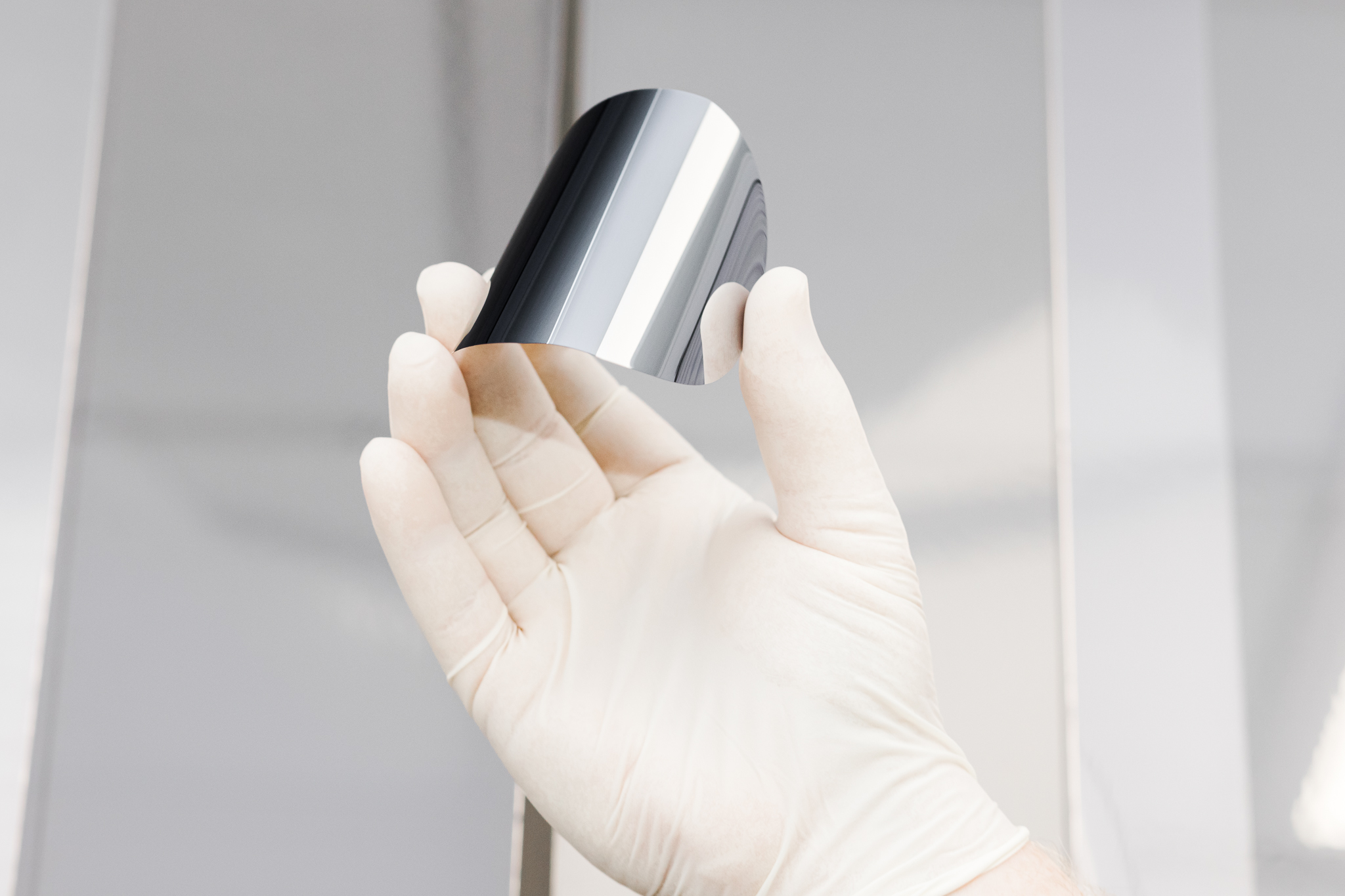
Grinding exposes a wafer to an abrasive-containing surface, like a grinding wheel, which removes material through direct engagement with that surface. Lapping works differently: the wafer contacts a flat lapping plate, typically cast iron, while a slurry of loose abrasive and carrier fluid is fed between the two.
That distinction matters because lapping generally provides better planarization than grinding, correcting variation across the wafer surface rather than just removing bulk material.
Since lapping quality has a direct effect on how much work polishing has to do afterward, it is worth asking a supplier how they control plate flatness, how often plates are conditioned, and what abrasive grit sequence they use for your specific material.
A supplier who can answer these questions specifically, rather than describing lapping in general terms, is more likely to deliver consistent results from batch to batch.
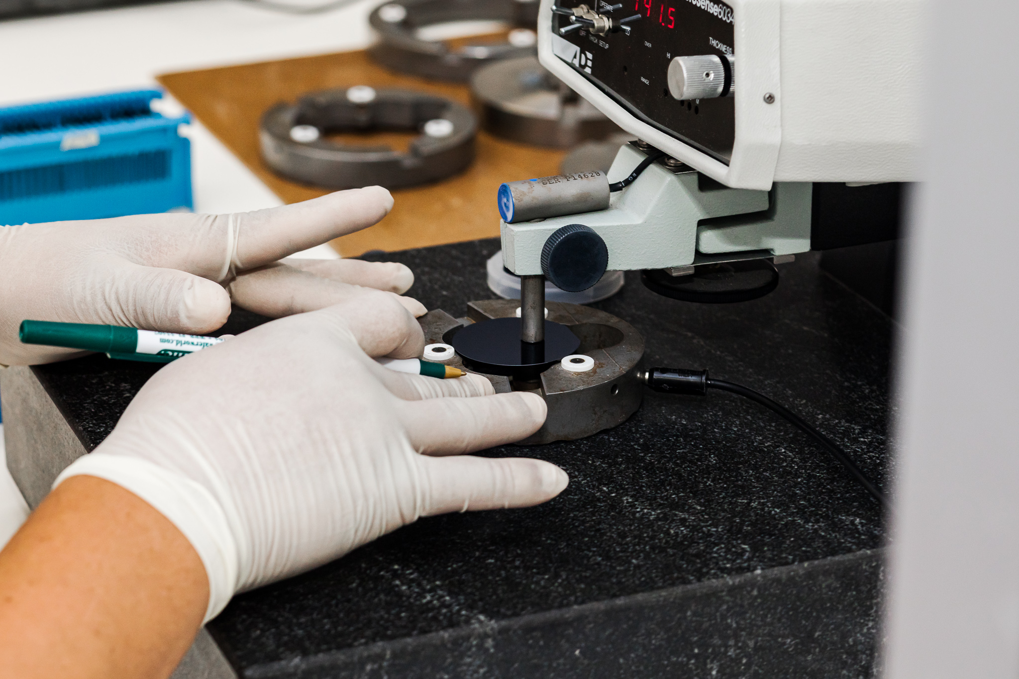
Consistent lapping results depend on tightly controlled equipment and process conditions. Wafer World maintains that control across silicon and compound semiconductor materials. Request a quote and our team can walk through the lapping and finishing specifications your project needs.