
The world has changed considerably over the past few years. If you showed a graphic designer from the 2000s the animations we see today, they’d believe you spent months working on them—if you told them an AI generator created them in seconds, they may throw their very heavy Mac computers through the window. Image generators have grown so rapidly these past two decades that it can be hard to overlook the role wafer manufacturing has played.
Many AI platforms require a lot of power to generate images, and that’s where semiconductors enter the picture. Various types of wafers power these complex systems.
EMBEB:
AI image generators, such as those powering tools like DALL·E, Midjourney, and Stable Diffusion, rely on high-performance computing hardware to process and generate complex images from text prompts.
At the heart of this hardware are semiconductor wafers—thin slices of crystalline material used to fabricate integrated circuits. These wafers are the foundational building blocks for the processors (such as GPUs, TPUs, and custom AI chips) that drive modern AI workloads.
The types of wafers used for AI image generators can be broadly categorized based on material, process technology, and intended chip function.
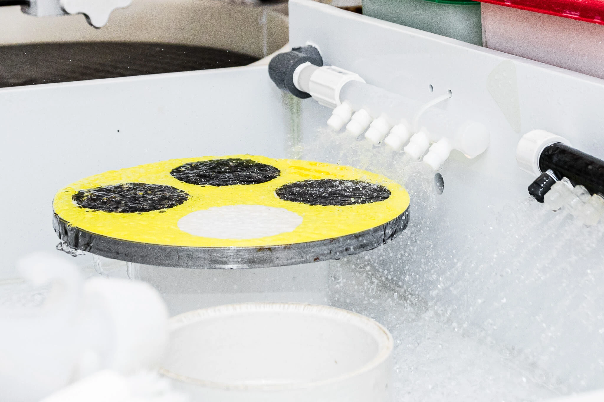
Silicon wafers are the most commonly used wafers in AI hardware. Due to its abundance and excellent electrical properties, silicon is the standard material for making the vast majority of integrated circuits.
These wafers are used to create general-purpose processors (CPUs), graphics processing units (GPUs), and application-specific integrated circuits (ASICs) used in AI image generation.
Advanced AI models require immense parallel computing power, which is typically provided by GPUs made by companies like NVIDIA and AMD. These GPUs are fabricated on high-purity silicon wafers using advanced process nodes (e.g., 5nm or 7nm), allowing for high transistor density, improved energy efficiency, and better performance.
While less common in AI-specific applications, compound semiconductors like Silicon Carbide (SiC) or Gallium Nitride (GaN) are sometimes used in power electronics that support AI systems, such as data center power supplies.
These materials are not typically used to fabricate the actual AI-processing chips. Their role is more supportive, helping to manage the massive energy requirements of AI infrastructure.
The performance of AI chips is also influenced by the wafer size and the process node used during manufacturing. Modern AI chips are typically produced on 300mm (12-inch) wafers, which allow foundries to fabricate more chips per wafer, reducing the cost per unit.
Process nodes such as 7nm, 5nm, and even 3nm (as used by companies like TSMC and Samsung) are critical for packing billions of transistors onto a single chip, which is necessary for running large-scale image generation models efficiently.
In cutting-edge AI chips, wafer-level technologies are used for advanced packaging. These approaches allow multiple dies (sometimes fabricated using different wafers or materials) to be integrated into a single package.
For example, high-bandwidth memory (HBM) dies might be stacked with logic dies to improve data throughput, which is essential for AI tasks.

As artificial intelligence (AI) image generators become more advanced, the demand for powerful hardware grows. However, producing wafers that can meet the unique demands of AI workloads presents several significant challenges.
One of the biggest challenges is the complexity of producing advanced wafers. AI chips require cutting-edge process nodes (such as 7 nm, 5 nm, and even 3 nm), which are extremely difficult to manufacture.
The smaller the transistor size, the more precision is required in lithography, layering, and doping processes. These advanced nodes also have higher defect rates, meaning more wafers must be discarded, increasing production costs.
Developing and producing AI-specific chips on advanced wafers is incredibly expensive. Building a modern semiconductor fabrication plant (fab) costs billions of dollars, and each wafer can cost thousands before even factoring in packaging and testing.
Since AI image generators often require clusters of GPUs or TPUs working in parallel, the hardware demand multiplies quickly.
AI image generation is highly compute-intensive and requires massive data processing. This leads to substantial heat generation and power consumption in chips fabricated on wafers. Managing heat across billions of transistors on a small surface area is a major challenge.
Wafers for AI chips depend on a complex and fragile global supply chain. Many materials, such as high-purity silicon, rare earth elements, and advanced photolithography equipment—are sourced from limited regions.
Geopolitical tensions, natural disasters, or trade restrictions can significantly disrupt supply.
As AI workloads scale, more wafers and chips must be kept up. However, not every wafer yields fully functional chips. Even small defects can make a chip unusable. Maintaining high yields while producing wafers at scale is a constant challenge, especially at advanced nodes.
There’s more to AI than software and code. These systems rely on high-performance processors like GPUs (Graphics Processing Units), TPUs (Tensor Processing Units), and other AI accelerators built using semiconductor wafers. Of course, using semiconductor wafers in AI image generators brings major challenges in manufacturing complexity, cost, thermal performance, supply chain stability, and scalability.
Overcoming these issues is essential to supporting the continued growth of AI technology and making powerful image generation accessible and sustainable. Would you like to learn more about the uses of semiconductors? Contact Wafer World for help!


