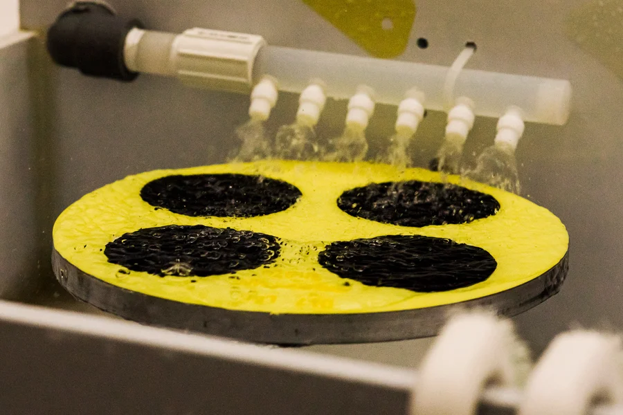
When applications require tight dimensional control, a wafer’s overall geometry deserves as much attention as its surface finish. Evaluating ultra flat wafers involves looking beyond whether a surface appears smooth. Thickness consistency, bow, warp, measurement conditions, and handling can all influence whether a substrate meets the dimensional requirements established for a particular application.
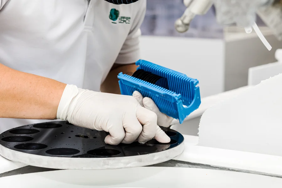
One important measurement is total thickness variation, commonly called TTV. SEMI standards define TTV as the difference between the maximum and minimum thickness values within a specified area of a wafer. This measurement helps describe how consistently the two wafer surfaces relate to each other across the measured region.
TTV should not be confused with surface roughness. A wafer may have a highly polished surface while still showing thickness variation across its diameter. For applications with demanding dimensional requirements, these characteristics need to be evaluated separately rather than treated as interchangeable indicators of quality.
Bow and warp provide additional information about wafer geometry. SEMI measurement standards distinguish these parameters because they describe different aspects of wafer shape. Bow relates to the displacement of the wafer’s median surface at its center relative to a reference plane. Warp considers variations of that median surface across the wafer.
Together, these measurements can provide a more complete picture than thickness alone.
Flatness values only become useful when the measurement method is clearly understood. The way a wafer is supported, the area being evaluated, and the reference plane used during measurement can affect how geometric characteristics are reported.
When reviewing specifications, it helps to consider:
These details make it easier to compare specifications accurately, rather than relying on a single flatness number without context.
Dimensional quality does not exist independently of surface condition. Particles, scratches, residues, and handling damage can affect a wafer’s suitability even when its geometric measurements fall within specified limits.
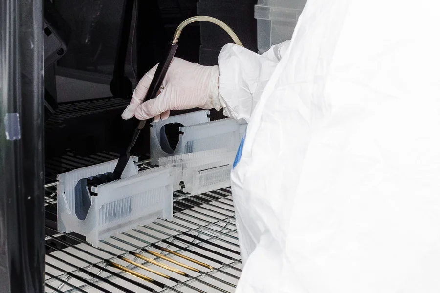
Careful packaging and handling are therefore part of maintaining the condition established during manufacturing and inspection. The National Institute of Standards and Technology notes that particles and other contaminants are important concerns in semiconductor wafer processing. Keeping wafers protected from unnecessary contact and contamination helps preserve their prepared surfaces before subsequent use.
There is no single flatness value that automatically defines the right wafer for every application. Requirements depend on the process, equipment, wafer dimensions, and intended use. A useful quality assessment considers multiple specifications together and confirms that measurement terminology is consistent between the supplier and customer.
Choosing ultra flat wafers starts with understanding which dimensional and surface characteristics matter for your application. Wafer World can help you review available wafer specifications and discuss substrate requirements without reducing quality to a single measurement. Contact us to schedule a consultation and explore wafer options suited to your process.




